1. Arria® 10 Transceiver PHY Overview
2. Implementing Protocols in Arria 10 Transceivers
3. PLLs and Clock Networks
4. Resetting Transceiver Channels
5. Arria 10 Transceiver PHY Architecture
6. Reconfiguration Interface and Dynamic Reconfiguration
7. Calibration
8. Analog Parameter Settings
9. Debugging Transceiver Toolkit
2.1. Transceiver Design IP Blocks
2.2. Transceiver Design Flow
2.3. Arria® 10 Transceiver Protocols and PHY IP Support
2.4. Using the Arria® 10 Transceiver Native PHY IP Core
2.5. Interlaken
2.6. Ethernet
2.7. PCI Express* (PIPE)
2.8. CPRI
2.9. Other Protocols
2.10. Simulating the Transceiver Native PHY IP Core
2.11. Implementing Protocols in Arria® 10 Transceivers Revision History
2.2.1. Select and Instantiate the PHY IP Core
2.2.2. Configure the PHY IP Core
2.2.3. Generate the PHY IP Core
2.2.4. Select the PLL IP Core
2.2.5. Configure the PLL IP Core
2.2.6. Generate the PLL IP Core
2.2.7. Reset Controller
2.2.8. Create Reconfiguration Logic
2.2.9. Connect the PHY IP to the PLL IP Core and Reset Controller
2.2.10. Connect Datapath
2.2.11. Make Analog Parameter Settings
2.2.12. Compile the Design
2.2.13. Verify Design Functionality
2.4.1. Presets
2.4.2. General and Datapath Parameters
2.4.3. PMA Parameters
2.4.4. Enhanced PCS Parameters
2.4.5. Standard PCS Parameters
2.4.6. PCS Direct
2.4.7. Dynamic Reconfiguration Parameters
2.4.8. PMA Ports
2.4.9. Enhanced PCS Ports
2.4.10. Standard PCS Ports
2.4.11. IP Core File Locations
2.4.12. Unused Transceiver RX Channels
2.4.13. Unsupported Features
2.6.1. Gigabit Ethernet (GbE) and GbE with IEEE 1588v2
2.6.2. 10GBASE-R, 10GBASE-R with IEEE 1588v2, and 10GBASE-R with FEC Variants
2.6.3. 10GBASE-KR PHY IP Core
2.6.4. 1-Gigabit/10-Gigabit Ethernet (GbE) PHY IP Core
2.6.5. 1G/2.5G/5G/10G Multi-rate Ethernet PHY Intel® FPGA IP Core
2.6.6. XAUI PHY IP Core
2.6.7. Acronyms
2.6.1.1. 8B/10B Encoding for GbE, GbE with IEEE 1588v2
2.6.1.2. Word Alignment for GbE, GbE with IEEE 1588v2
2.6.1.3. 8B/10B Decoding for GbE, GbE with IEEE 1588v2
2.6.1.4. Rate Match FIFO for GbE
2.6.1.5. How to Implement GbE, GbE with IEEE 1588v2 in Arria® 10 Transceivers
2.6.1.6. Native PHY IP Parameter Settings for GbE and GbE with IEEE 1588v2
2.6.2.1. The XGMII Clocking Scheme in 10GBASE-R
2.6.2.2. How to Implement 10GBASE-R, 10GBASE-R with IEEE 1588v2, and 10GBASE-R with FEC in Arria 10 Transceivers
2.6.2.3. Native PHY IP Parameter Settings for 10GBASE-R, 10GBASE-R with IEEE 1588v2, and 10GBASE-R with FEC
2.6.2.4. Native PHY IP Ports for 10GBASE-R and 10GBASE-R with IEEE 1588v2 Transceiver Configurations
2.6.3.1. 10GBASE-KR PHY Release Information
2.6.3.2. 10GBASE-KR PHY Performance and Resource Utilization
2.6.3.3. 10GBASE-KR Functional Description
2.6.3.4. Parameterizing the 10GBASE-KR PHY
2.6.3.5. 10GBASE-KR PHY Interfaces
2.6.3.6. Avalon® Memory-Mapped Interface Registers
2.6.3.7. Creating a 10GBASE-KR Design
2.6.3.8. Design Example
2.6.3.9. Simulation Support
2.6.4.1. 1G/10GbE PHY Release Information
2.6.4.2. 1G/10GbE PHY Performance and Resource Utilization
2.6.4.3. 1G/10GbE PHY Functional Description
2.6.4.4. Clock and Reset Interfaces
2.6.4.5. Parameterizing the 1G/10GbE PHY
2.6.4.6. 1G/10GbE PHY Interfaces
2.6.4.7. Avalon® Memory-Mapped Interface Registers
2.6.4.8. Creating a 1G/10GbE Design
2.6.4.9. Design Guidelines
2.6.4.10. Channel Placement Guidelines
2.6.4.11. Design Example
2.6.4.12. Simulation Support
2.6.4.13. TimeQuest Timing Constraints
2.6.6.1. Transceiver Datapath in a XAUI Configuration
2.6.6.2. XAUI Supported Features
2.6.6.3. XAUI PHY Release Information
2.6.6.4. XAUI PHY Device Family Support
2.6.6.5. Transceiver Clocking and Channel Placement Guidelines in XAUI Configuration
2.6.6.6. XAUI PHY Performance and Resource Utilization
2.6.6.7. Parameterizing the XAUI PHY
2.6.6.8. XAUI PHY Ports
2.6.6.9. XAUI PHY Interfaces
2.6.6.10. XAUI PHY Register Interface and Register Descriptions
2.6.6.11. XAUI PHY Timing Analyzer SDC Constraint
2.7.1. Transceiver Channel Datapath for PIPE
2.7.2. Supported PIPE Features
2.7.3. How to Connect TX PLLs for PIPE Gen1, Gen2, and Gen3 Modes
2.7.4. How to Implement PCI Express* (PIPE) in Arria 10 Transceivers
2.7.5. Native PHY IP Parameter Settings for PIPE
2.7.6. fPLL IP Parameter Core Settings for PIPE
2.7.7. ATX PLL IP Parameter Core Settings for PIPE
2.7.8. Native PHY IP Ports for PIPE
2.7.9. fPLL Ports for PIPE
2.7.10. ATX PLL Ports for PIPE
2.7.11. Preset Mappings to TX De-emphasis
2.7.12. How to Place Channels for PIPE Configurations
2.7.13. PHY IP Core for PCIe* (PIPE) Link Equalization for Gen3 Data Rate
2.7.14. Using Transceiver Toolkit (TTK)/System Console/Reconfiguration Interface to manually tune Arria® 10 PCIe designs (Hard IP(HIP) and PIPE) (For debug only)
2.7.2.1.1. Dynamic Switching Between Gen1 (2.5 Gbps) and Gen2 (5 Gbps)
2.7.2.1.2. Transmitter Electrical Idle Generation
2.7.2.1.3. Power State Management
2.7.2.1.4. 8B/10B Encoder Usage for Compliance Pattern Transmission Support
2.7.2.1.5. Receiver Status
2.7.2.1.6. Receiver Detection
2.7.2.1.7. Gen1 and Gen2 Clock Compensation
2.7.2.1.8. PCIe* Reverse Parallel Loopback
2.9.1. Using the 'Basic (Enhanced PCS)' and 'Basic with KR FEC' Configurations of Enhanced PCS
2.9.2. Using the Basic/Custom, Basic/Custom with Rate Match Configurations of Standard PCS
2.9.3. Design Considerations for Implementing Arria 10 GT Channels
2.9.4. How to Implement PCS Direct Transceiver Configuration Rule
2.9.1.1. How to Implement the Basic (Enhanced PCS) and Basic with KR FEC Transceiver Configuration Rules in Arria 10 Transceivers
2.9.1.2. Native PHY IP Parameter Settings for Basic (Enhanced PCS) and Basic with KR FEC
2.9.1.3. How to Enable Low Latency in Basic Enhanced PCS
2.9.1.4. Enhanced PCS FIFO Operation
2.9.1.5. TX Data Bitslip
2.9.1.6. TX Data Polarity Inversion
2.9.1.7. RX Data Bitslip
2.9.1.8. RX Data Polarity Inversion
2.9.2.1. Word Aligner Manual Mode
2.9.2.2. Word Aligner Synchronous State Machine Mode
2.9.2.3. RX Bit Slip
2.9.2.4. RX Polarity Inversion
2.9.2.5. RX Bit Reversal
2.9.2.6. RX Byte Reversal
2.9.2.7. Rate Match FIFO in Basic (Single Width) Mode
2.9.2.8. Rate Match FIFO Basic (Double Width) Mode
2.9.2.9. 8B/10B Encoder and Decoder
2.9.2.10. 8B/10B TX Disparity Control
2.9.2.11. How to Enable Low Latency in Basic
2.9.2.12. TX Bit Slip
2.9.2.13. TX Polarity Inversion
2.9.2.14. TX Bit Reversal
2.9.2.15. TX Byte Reversal
2.9.2.16. How to Implement the Basic, Basic with Rate Match Transceiver Configuration Rules in Arria® 10 Transceivers
2.9.2.17. Native PHY IP Parameter Settings for Basic, Basic with Rate Match Configurations
3.1. PLLs
3.2. Input Reference Clock Sources
3.3. Transmitter Clock Network
3.4. Clock Generation Block
3.5. FPGA Fabric-Transceiver Interface Clocking
3.6. Transmitter Data Path Interface Clocking
3.7. Receiver Data Path Interface Clocking
3.8. Unused/Idle Clock Line Requirements
3.9. Channel Bonding
3.10. PLL Feedback and Cascading Clock Network
3.11. Using PLLs and Clock Networks
3.12. PLLs and Clock Networks Revision History
4.1. When Is Reset Required?
4.2. Transceiver PHY Implementation
4.3. How Do I Reset?
4.4. Using the Transceiver PHY Reset Controller
4.5. Using a User-Coded Reset Controller
4.6. Combining Status or PLL Lock Signals
4.7. Timing Constraints for Bonded PCS and PMA Channels
4.8. Resetting Transceiver Channels Revision History
4.3.2.1. Recommended Reset Sequence
4.3.2.2. Resetting the Transmitter During Device Operation
4.3.2.3. Resetting the Receiver During Device Operation
4.3.2.4. Dynamic Reconfiguration of Transmitter Channel Using the Acknowledgment Model
4.3.2.5. Dynamic Reconfiguration of Receiver Channel Using the Acknowledgment Model
5.1.5.1. Programmable Common Mode Voltage (VCM)
5.1.5.2. Programmable Differential On-Chip Termination (OCT)
5.1.5.3. Signal Detector
5.1.5.4. Continuous Time Linear Equalization (CTLE)
5.1.5.5. Variable Gain Amplifier (VGA)
5.1.5.6. Decision Feedback Equalization (DFE)
5.1.5.7. How to Enable CTLE and DFE
5.2.1.1. Enhanced PCS TX FIFO
5.2.1.2. Interlaken Frame Generator
5.2.1.3. Interlaken CRC-32 Generator
5.2.1.4. 64B/66B Encoder and Transmitter State Machine (TX SM)
5.2.1.5. Pattern Generators
5.2.1.6. Scrambler
5.2.1.7. Interlaken Disparity Generator
5.2.1.8. TX Gearbox, TX Bitslip and Polarity Inversion
5.2.1.9. KR FEC Blocks
5.2.2.1. RX Gearbox, RX Bitslip, and Polarity Inversion
5.2.2.2. Block Synchronizer
5.2.2.3. Interlaken Disparity Checker
5.2.2.4. Descrambler
5.2.2.5. Interlaken Frame Synchronizer
5.2.2.6. 64B/66B Decoder and Receiver State Machine (RX SM)
5.2.2.7. Pseudo Random Pattern Verifier
5.2.2.8. 10GBASE-R Bit-Error Rate (BER) Checker
5.2.2.9. Interlaken CRC-32 Checker
5.2.2.10. Enhanced PCS RX FIFO
5.2.2.11. RX KR FEC Blocks
5.3.1.3.1. 8B/10B Encoder Control Code Encoding
5.3.1.3.2. 8B/10B Encoder Reset Condition
5.3.1.3.3. 8B/10B Encoder Idle Character Replacement Feature
5.3.1.3.4. 8B/10B Encoder Current Running Disparity Control Feature
5.3.1.3.5. 8B/10B Encoder Bit Reversal Feature
5.3.1.3.6. 8B/10B Encoder Byte Reversal Feature
5.3.2.1.1. Word Aligner Bit Slip Mode
5.3.2.1.2. Word Aligner Manual Mode
5.3.2.1.3. Word Aligner Synchronous State Machine Mode
5.3.2.1.4. Word Aligner Deterministic Latency Mode
5.3.2.1.5. Word Aligner Pattern Length for Various Word Aligner Modes
5.3.2.1.6. Word Aligner RX Bit Reversal Feature
5.3.2.1.7. Word Aligner RX Byte Reversal Feature
6.1. Reconfiguring Channel and PLL Blocks
6.2. Interacting with the Reconfiguration Interface
6.3. Configuration Files
6.4. Multiple Reconfiguration Profiles
6.5. Embedded Reconfiguration Streamer
6.6. Arbitration
6.7. Recommendations for Dynamic Reconfiguration
6.8. Steps to Perform Dynamic Reconfiguration
6.9. Direct Reconfiguration Flow
6.10. Native PHY IP or PLL IP Core Guided Reconfiguration Flow
6.11. Reconfiguration Flow for Special Cases
6.12. Changing PMA Analog Parameters
6.13. Ports and Parameters
6.14. Dynamic Reconfiguration Interface Merging Across Multiple IP Blocks
6.15. Embedded Debug Features
6.16. Using Data Pattern Generators and Checkers
6.17. Timing Closure Recommendations
6.18. Unsupported Features
6.19. Arria® 10 Transceiver Register Map
6.20. Reconfiguration Interface and Dynamic Revision History
8.1. Making Analog Parameter Settings using the Assignment Editor
8.2. Updating Quartus Settings File with the Known Assignment
8.3. Analog Parameter Settings List
8.4. Receiver General Analog Settings
8.5. Receiver Analog Equalization Settings
8.6. Transmitter General Analog Settings
8.7. Transmitter Pre-Emphasis Analog Settings
8.8. Transmitter VOD Settings
8.9. Dedicated Reference Clock Settings
8.10. Unused Transceiver RX Channels Settings
8.11. Analog Parameter Settings Revision History
8.7.1. XCVR_A10_TX_PRE_EMP_SIGN_PRE_TAP_1T
8.7.2. XCVR_A10_TX_PRE_EMP_SIGN_PRE_TAP_2T
8.7.3. XCVR_A10_TX_PRE_EMP_SIGN_1ST_POST_TAP
8.7.4. XCVR_A10_TX_PRE_EMP_SIGN_2ND_POST_TAP
8.7.5. XCVR_A10_TX_PRE_EMP_SWITCHING_CTRL_PRE_TAP_1T
8.7.6. XCVR_A10_TX_PRE_EMP_SWITCHING_CTRL_PRE_TAP_2T
8.7.7. XCVR_A10_TX_PRE_EMP_SWITCHING_CTRL_1ST_POST_TAP
8.7.8. XCVR_A10_TX_PRE_EMP_SWITCHING_CTRL_2ND_POST_TAP
2.9.3.4. How to Implement Designs for Data Rates Above 17.4 Gbps Using Enhanced PCS in Low Latency Mode
- You should be familiar with the Enhanced PCS and PMA architecture, PLL architecture, and the reset controller.
- Make sure you have selected an Arria 10 GT device for the project
- Select Tools > IP Catalog > Interface Protocols > Transceiver PHY > Arria 10 Transceiver Native PHY. Refer to Select and Instantiate the PHY IP Core for detailed steps.
- Set VCCR_GXB and VCCT_GXB to 1.1V. Note these settings are overridden by the QSF file settings which should also be set to 1.1V. QII makes sure the actual voltage prescribed is in line with pin connection guidelines and the Arria10 Data Sheet.
- Select Basic (Enhanced PCS) from the Transceiver configuration rules list located under Datapath Options.
- Use the parameter values in the tables in Transceiver Native PHY IP Parameters Settings for Basic (Enhanced PCS) and Basic with KR FEC for each input of the Arria 10 Transceiver Native PHY Parameter Editor as a starting point. Or, you can use the protocol presets described in Transceiver Native PHY Presets. You can then modify the settings to meet your specific requirements.
- Ensure that the data rate is set to 25781.25 Mbps. To achieve the higher data rates, use Enhanced PCS basic mode with the low latency option unchecked. Select a CDR reference clock to match your data rate. Use Phase compensation FIFO modes.
- Make sure DFE is disabled from Rx PMA settings.
- Set the Enhanced PCS / PMA interface width to 64 bits.
- Set the FPGA fabric / Enhanced PCS interface width to 64 bits.
- You can enable RX/TX FIFO double width mode to create a FPGA fabric / PCS interface width of 128 bits.
- Click Finish to generate the Native PHY IP (this is your RTL file).
Figure 162. Signals and Ports of the Native PHY for Basic (Enhanced PCS) Transceiver Configuration Rule for Data Rates Above 17.4 Gbps and FPGA Fabric / PCS Interface width of 128 bits
- Select Tools > IP Catalog > Basic Functions > Clocks > PLLs and Resets > PLL > Arria 10 Transceiver ATX PLL. Refer to Instantiating the ATX PLL IP Core for detailed steps.
- Configure the ATX PLL IP using the Parameter Editor.
- Select the GT clock output buffer.
- Enable the PLL GT clock output port.
- Set the PLL output clock frequency to the Native PHY IP recommended frequency.
Figure 163. ATX PLL IP with GT Clock Lines Enabled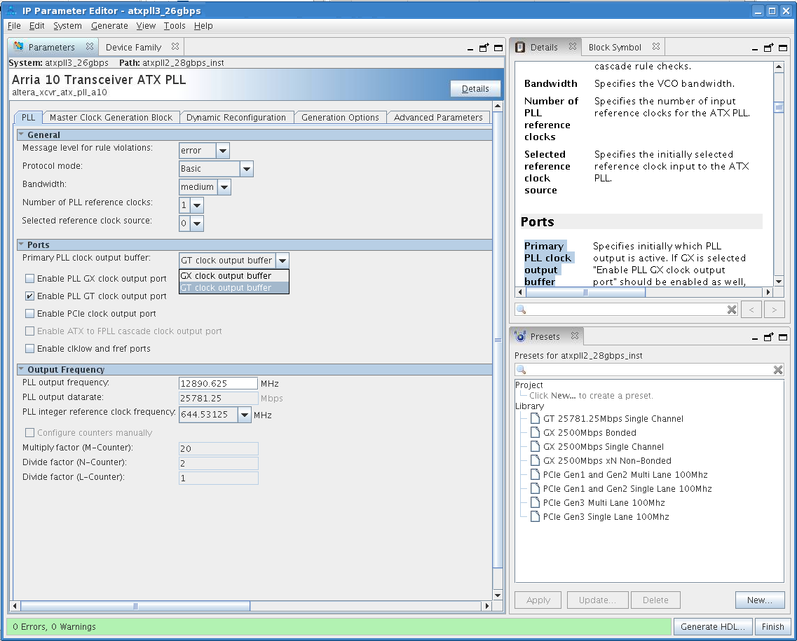
- Create a transceiver reset controller. Refer to Resetting Transceiver Channels for more details about configuring the reset IP core.
- Connect the Native PHY IP core to the PLL IP core and the reset controller.
The ATX PLL's port tx_serial_clk_gt represents the dedicated GT clock lines. Connect this port to the Native PHY IP core's tx_serial_clk0 port. The Quartus Prime software automatically uses the dedicated GT clocks instead of the x1 clock network.