3.1.1.2. Using the ATX PLL for GXT Channels
- Main ATX PLL is configured as a transmit PLL
- Adjacent top ATX PLL is configured as a GXT clock buffer, passing the center ATX PLL’s serial clock to the adjacent GXT channels
- Adjacent bottom ATX PLL is configured as a GXT clock buffer, passing the center ATX PLL’s serial clock to the adjacent GXT channels
No GXT clock buffer ATX PLLs are needed, if 2 GXT channels are required and they are adjacent (channels 0 and 1 in a bank and the transmit ATX PLL is located in the bottom of the bank or channels 3 and 4 in a bank and the transmit ATX PLL is located in the top of the bank) to the transmit ATX PLL. The same rule applies, if a single GXT channel is required.
A single GXT clock buffer ATX PLL is needed, if 4 GXT channels are required and they are adjacent (channels 0, 1, 3 and 4 in a bank or channels 0 and 1 in a bank and channels 3 and 4 in the bank below). The transmit ATX PLL can be the ATX PLL adjacent to the top or bottom 2 GXT channels. The same rule applies, if 3 GXT channels are required.
The reference clock for GXT channels must be located in the same triplet as the master ATX PLL.
- tx_serial_clk_gxt output port on transmit and GXT clock buffer ATX PLLs. The tx_serial_clk_gxt connects to the tx_serial_clk port in the Stratix® 10 L-Tile/H-Tile Native PHY IP
- gxt_output_to_abv_atx output port on ATX PLLs configured as transmit PLLs, outputs the GXT serial clock to the above ATX PLL configured as a GXT clock buffer
- gxt_output_to_blw_atx output port on ATX PLLs configured as transmit PLLs, outputs the GXT serial clock to the below ATX PLL configured as a GXT clock buffer
- gxt_input_from_blw_atx input port on ATX PLLs configured as GXT clock buffer inputs the GXT serial clock from the below ATX PLL configured as a transmit PLL
- gxt_input_from_abv_atx input port on ATX PLLs configured as GXT clock buffer inputs the GXT serial clock from the above ATX PLL configured as a transmit PLL
Port gxt_output_to_abv_atx of the transmit ATX PLL needs to be connected to port gxt_input_from_blw_atx of the above GXT clock buffer ATX PLL.
Port gxt_output_to_blw_atx of the transmit ATX PLL needs to be connected to port gxt_input_from_abv_atx of the below GXT clock buffer ATX PLL.
- GXT transmit PLL with GXT clocks to adjacent GXT channels
- GXT transmit PLL with GXT clocks to GXT clock buffer ATX PLLs
- GXT transmit PLL with GXT clocks to adjacent GXT channels and GXT clock buffer ATX PLLs
- GXT clock buffer ATX PLL
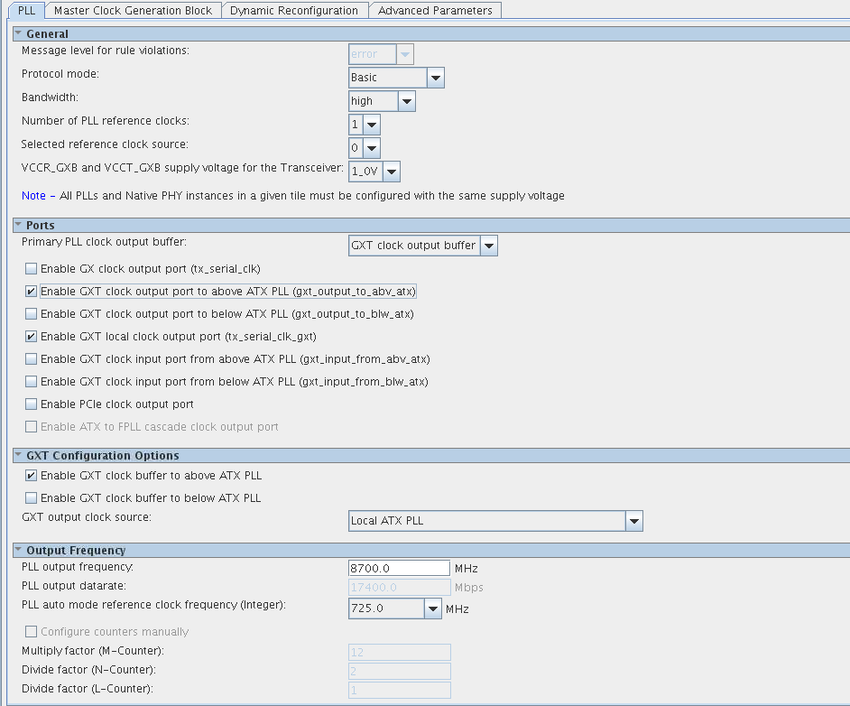
- Set the Primary PLL clock output buffer drop-down to GXT clock output buffer.
- Select the Enable GXT local clock output port (tx_serial_clk_gxt) checkbox.
- Set the GXT output clock source drop-down as Local ATX PLL.
- Set the ATX PLL input reference clock and datarate parameters.
- Set the Primary PLL clock output buffer drop-down to GXT clock output buffer.
- Select the Enable GXT clock output port to above ATX PLL (gxt_output_to_abv_atx), Enable GXT clock output port to below ATX PLL (gxt_output_to_blw_atx), or both checkbox.
- Select the Enable GXT clock buffer to above ATX PLL, Enable GXT clock buffer to below ATX PLL, or both checkbox.
- Set the GXT output clock source drop-down as Disabled.
- Set the ATX PLL input reference clock and datarate parameters.
- Set the Primary PLL clock output buffer drop-down to GXT clock output buffer.
- Select the Enable GXT local clock output port (tx_serial_clk_gxt) checkbox.
- Set the GXT output clock source drop-down as Local ATX PLL.
- Select the Enable GXT output port to above ATX PLL (gxt_output_to_abv_atx) or Enable GXT output port to below ATX PLL (gxt_output_to_blw_atx), or select both checkboxes if needed.
- Select the Enable GXT clock buffer to above ATX PLL, Enable GXT clock buffer, or both to above ATX PLL checkbox.
- Set the ATX PLL input reference clock and datarate parameters.
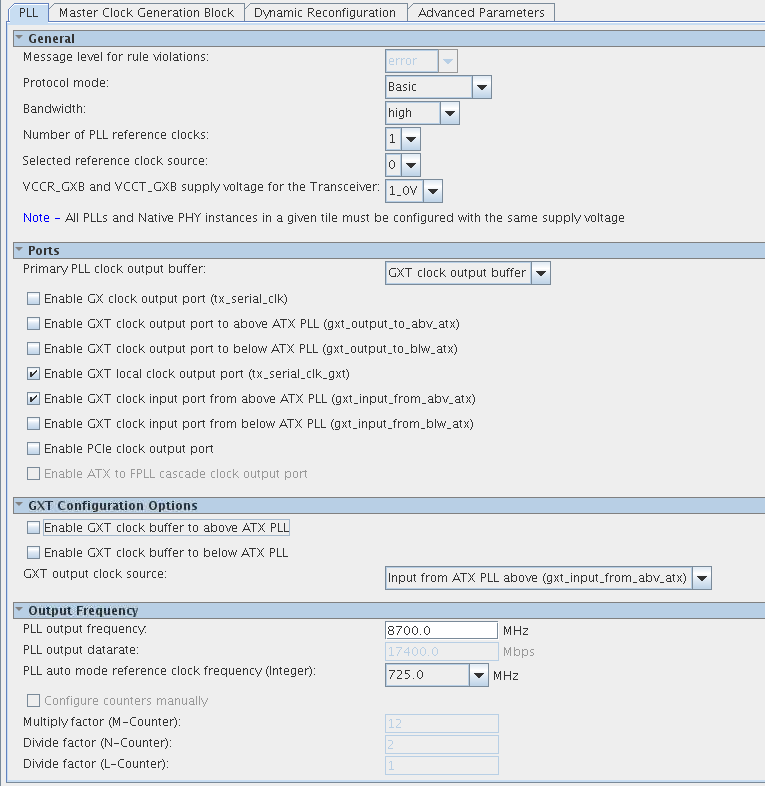
- Set the Primary PLL clock output buffer drop-down to GXT clock output buffer.
- Select the Enable GXT local clock output port (tx_serial_clk_gxt) checkbox.
- Select the Enable GXT clock input port from above ATX PLL (gxt_input_from_abv_atx) or Enable GXT clock input port from below ATX PLL (gxt_input_from_blw_atx) checkbox.
- Set the GXT output clock source drop-down as Input from ATX PLL above (gxt_input_from_abv_atx) or Input from ATX PLL below (gxt_input_from_blw_atx) to align with selection in step 3.
- The pll_refclk0 pin of the clock buffer ATX PLL IP can be connected to the REFCLK pin used by the main ATX PLL IP, if the GXT clock buffer ATX PLL is not reconfigured as a GXT transmit PLL or GX transmit PLL. It can also be left unconnected.
An ATX PLL can be reconfigured between modes, but all needed ports must be enabled in the instance.