External Memory Interface Handbook Volume 2: Design Guidelines: For UniPHY-based Device Families
1.2.2.3. Determining the CQ/CQn Arrival Time Skew
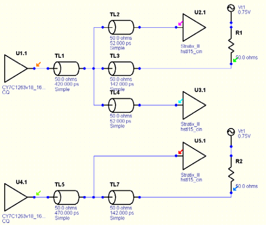
The following figure shows an example of a board topology comparing an emulated case where CQ is double-loaded and a non-emulated case where CQ only has a single load.
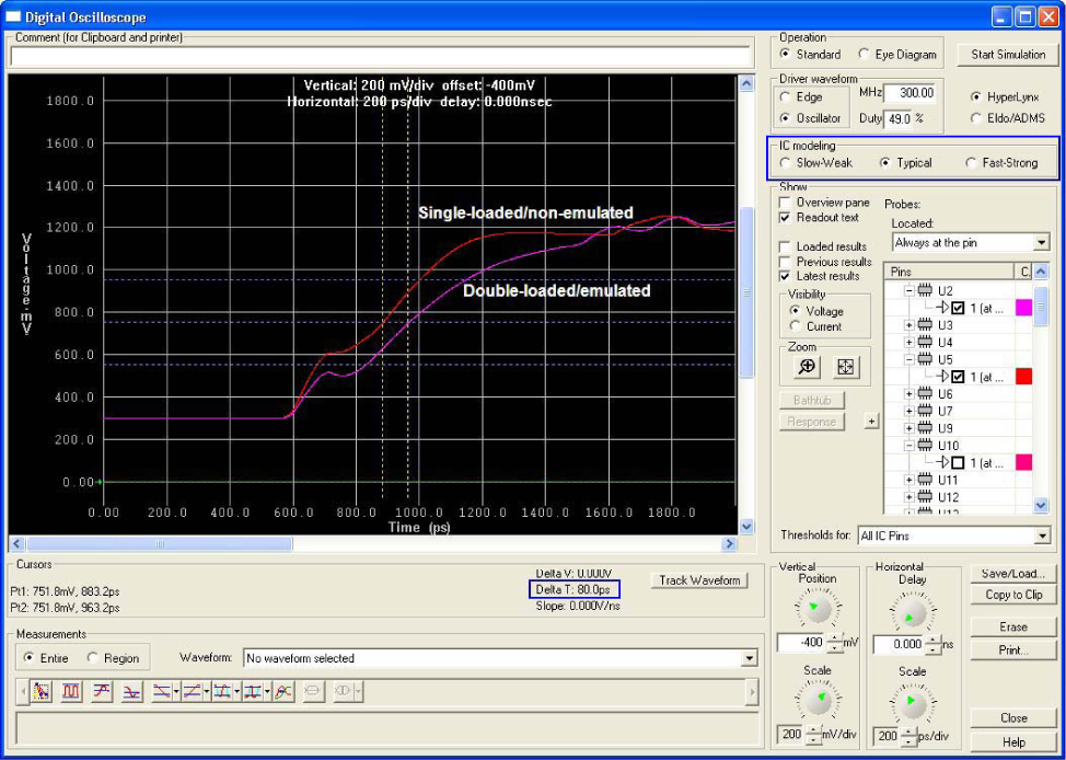
Run the simulation and look at the signal at the FPGA pin. The following figure shows an example of the simulation results from the preceding figure. As expected, the double-loaded emulated signal, in pink, arrives at the FPGA pin later than the single-loaded signal, in red. You then need to calculate the difference of this arrival time at VREF level (0.75 V in this case). Record the skew and rerun the simulation in the other two cases (slow-weak and fast-strong). To pick the largest and smallest skew to be included in Intel® Quartus® Prime timing analysis, follow these steps:
- Open the <variation_name>_report_timing.tcl and search for tmin_additional_dqs_variation.
- Set the minimum skew value from your board simulation to tmin_additional_dqs_variation.
- Set the maximum skew value from your board simulation to tmax_additional_dqs_variation.
- Save the .tcl file.