External Memory Interface Handbook Volume 2: Design Guidelines: For UniPHY-based Device Families
11.2.3. Additive Latency
You may issue the commands externally but the device holds the commands internally for the duration of additive latency before executing, to improve the system scheduling. The delay helps to avoid collision on the command bus and gaps in data input or output bursts. Additive latency allows the controller to issue the row and column address commands—activate, and read or write—in consecutive clock cycles, so that the controller need not hold the column address for several (tRCD) cycles. This gap between the activate and the read or write command can cause bubbles in the data stream.
The following figure shows an example of additive latency.
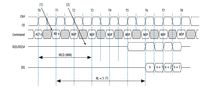
The following sequence of events describes the above figure:
- The controller issues a read or write command before the tRCD (MIN) requirement— additive latency less than or equal to tRCD (MIN).
- The controller holds the read or write command for the time defined by additive latency before issuing it internally to the SDRAM device.
Read latency = additive latency + CAS latency
Write latency = additive latency + CAS latency – tCK