External Memory Interfaces Intel® Stratix® 10 FPGA IP User Guide
A newer version of this document is available. Customers should click here to go to the newest version.
3.7.1. Restrictions on I/O Bank Usage for Intel® Stratix® 10 EMIF IP with HPS
The restrictions on I/O bank usage result from the Intel® Stratix® 10 HPS having hard-wired connections to the EMIF circuits in the I/O banks closest to the HPS. For any given EMIF configuration, the pin-out of the EMIF-to-HPS interface is fixed.
The following diagram illustrates the use of I/O banks and lanes for various EMIF-HPS data widths:
The HPS EMIF uses the closest located external memory interfaces I/O banks to connect to SDRAM.
The following diagram illustrates restrictions on I/O pin usage. Refer to the text following the diagram for a detailed explanation of these restrictions.
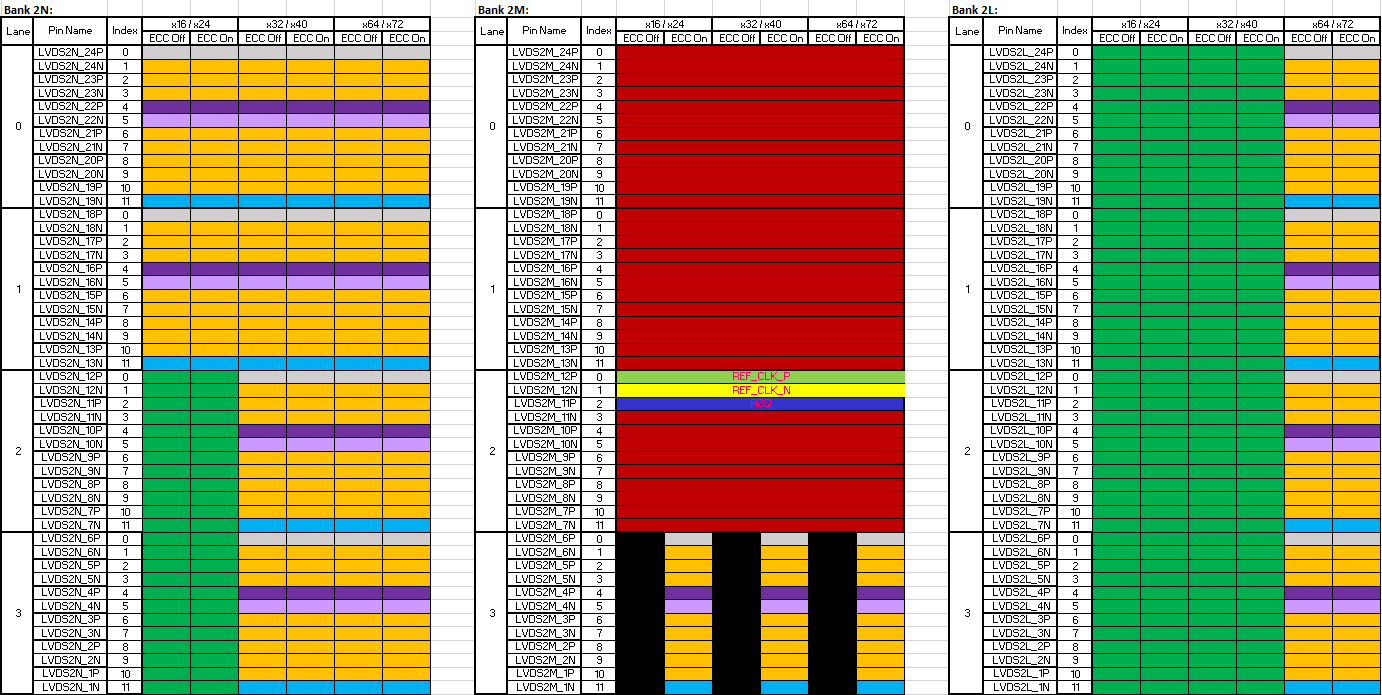
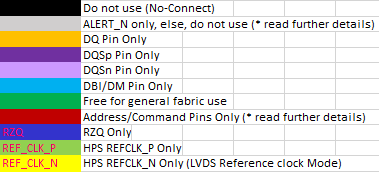
If no HPS EMIF is used in a system, the entire HPS EMIF bank can be used as FPGA general purpose I/O. If there is an HPS EMIF in a system, the unused HPS EMIF pins can be used as FPGA general purpose I/O, with the following restrictions:
- Bank 2M:
- Lane 3 of Bank 2M is used for data bits only when ECC mode is active. Whether ECC is active or not, you must not put general purpose I/Os in this lane.
- Lanes 2, 1, and 0 are used for SDRAM address and command. Unused pins in these lanes should not be used by the FPGA fabric, because their operation cannot be guaranteed.
- Bank 2N and Bank 2L :
- Lanes 3, 2, 1, and 0 are used for data bits.
- With 64-bit data widths, unused pins in these banks should not be used by the FPGA fabric, because their operation cannot be guaranteed.
- With 32-bit data widths, unused pins in Bank 2N should not be used by the FPGA fabric, because their operation cannot be guaranteed. Lanes 0-3 of bank 2L are not used by the HPS EMIF, therefore any pins within these lanes can be used by the FPGA fabric.
- With 16-bit data widths, Intel® Quartus® Prime assigns lane 0 and lane 1 as data lanes in bank 2N. Unused pins in these two lanes should not be used by the FPGA fabric, because their operation cannot be guaranteed. Lanes 2 and 3 are not used by the HPS EMIF, therefore pins within these lanes can be used by the FPGA fabric.
By default, the Intel® Stratix® 10 External Memory Interface for HPS IP core together with the Intel® Quartus® Prime Fitter automatically implements a starting point placement which you may need to modify. You must adhere to the following requirements, which are specific to HPS EMIF:
- Within a single data lane (which implements a single x8 DQS group):
- DQ pins must use pins at indices 1, 2, 3, 6, 7, 8, 9, 10. You may swap the locations between the DQ bits (that is, you may swap location of DQ[0] and DQ[3]) so long as the resulting pin-out uses pins at these indices only.
- DM/DBI pin must use pin at index 11. There is no flexibility.
- DQS and DQS# must use pins at index 4 and 5, respectively. There is no flexibility.
- Pin index 0 must have no connection, unless used for alert# or HPS REFCLK_P, or address/command, or general-purpose I/O, where allowed.
- The above figures show an overview of how the data lanes are used, depending on the width of the interface. The following table shows the I/O bank and I/O lanes that you must use, depending on the width and configuration of the interface.
Configuration DQS Group Placement 16 bit Must be placed in I/O lanes 0 and 1 of 2N. 16 bit + ECC Must be placed in I/O lanes 0 and 1 of 2N and I/O lane 3 of 2M. 32 bit Must be placed in 2N. 32 bit + ECC Must be placed in 2N and I/O lane 3 of 2M. 64 bit Must be placed in 2N and 2L. 64 bit + ECC Must be placed in 2N, 2L, and I/O lane 3 of 2M. Note:- In all cases, the DQS groups can be swapped around in the I/O banks shown. There is no requirement for the ECC DQS group to be placed in bank 2M.
- I/O lane 3 of bank 2M cannot be used if ECC is turned off. You must not put general purpose I/Os in lane 3 of bank 2M.
- You must not change placement of the address and command pins from the default placement in I/O bank 2M.
- The alert# pin must be at index 0 (of any lane of any bank) and must be grouped with its Intel® Quartus® Prime software-assigned DQS group, or must be in any unused pin within address and command section. Bank 2N, lane 0, index 0 or bank 2N, lane 1, index 0 are the recommended locations for alert# for new designs. This allows for maximum flexibility of different interface widths. Existing (working) designs with alert#, on unused address and command pins, or in other data I/O lanes at index 0, is allowed.
- The PLL reference clock must be placed in I/O bank 2M with the address and command pins. Failure to do this results in device configuration problems. The PLL reference clock must be running at the correct frequency before device configuration occurs.
- The RZQ pin must be placed in I/O bank 2M with the address and command pins. Failure to do this will cause Fitter or device configuration problems.
To override the default generated pin assignments, comment out the relevant HPS_LOCATION assignments in the .qip file, and add your own location assignments (using set_location_assignment) in the .qsf file.