External Memory Interfaces Intel® Stratix® 10 FPGA IP User Guide
A newer version of this document is available. Customers should click here to go to the newest version.
7.5.2.4. Guidelines for Calculating DDR4 Channel Signal Integrity
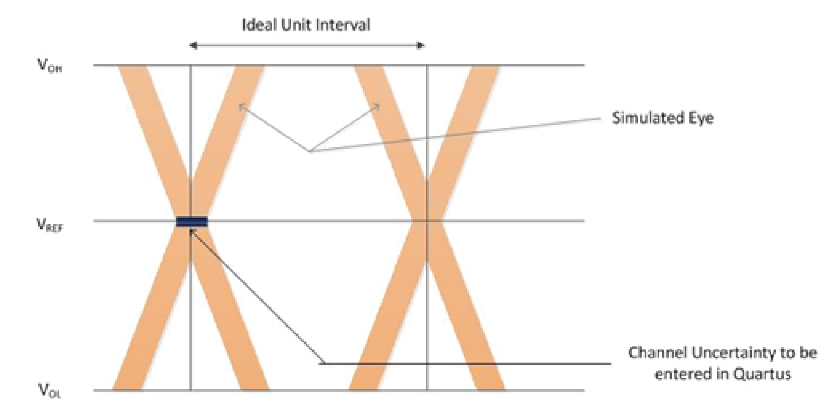
Address and Command ISI and Crosstalk
Simulate the address/command and control signals and capture eye at the DRAM pins, using the memory clock as the trigger for the memory interface's address/command and control signals. Measure the setup and hold channel losses at the voltage thresholds mentioned in the memory vendor's data sheet. For optimal address/command signal integrity, you should simulate both slow and fast slew rate settings.
Address and command channel loss = Measured loss on the setup side + measured loss on the hold side.
VREF = VDD/2 = 0.60 V for address/command for DDR4.
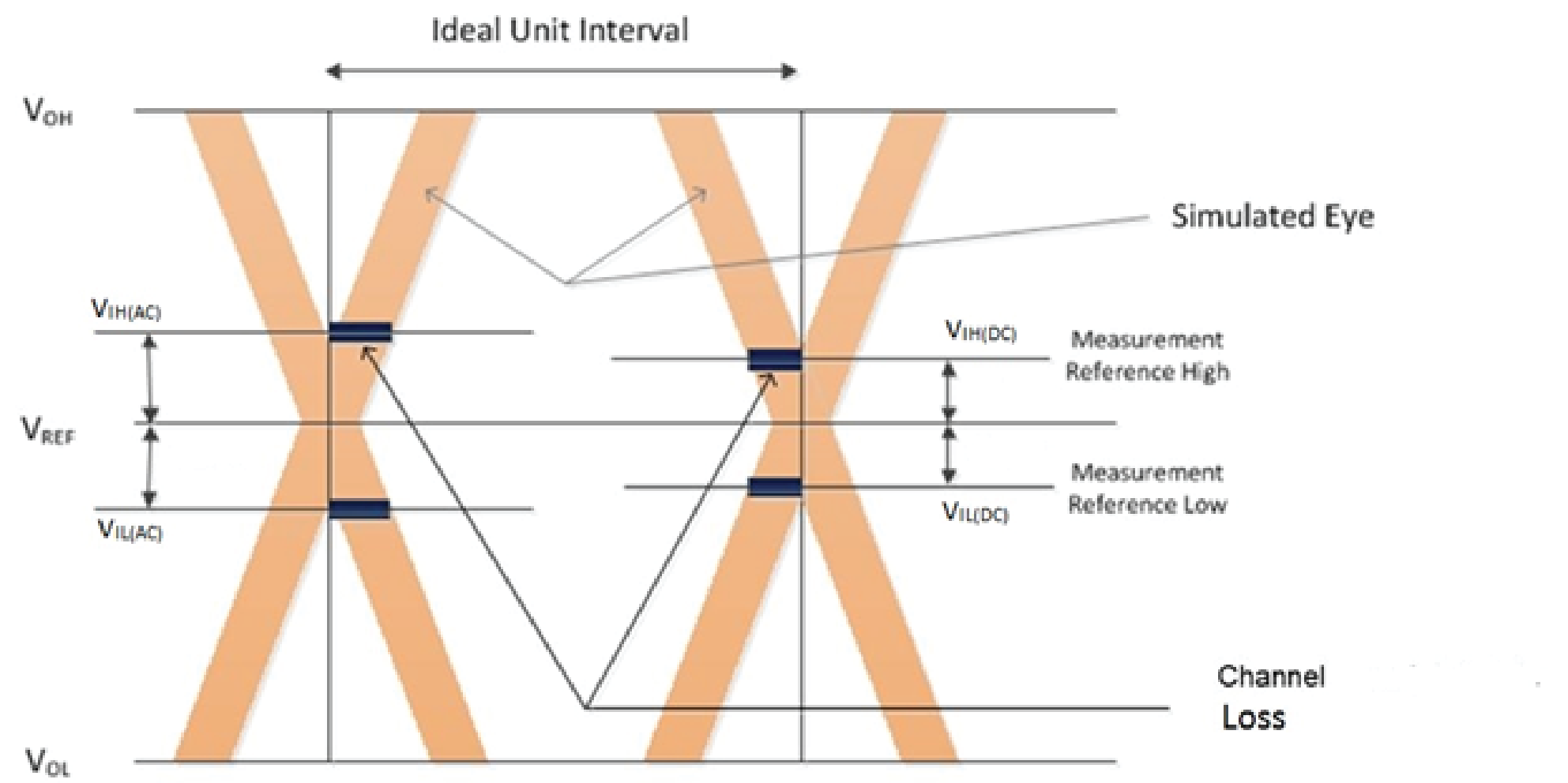
You should select the VIH and VIL voltage levels appropriately for the DDR4 memory device that you are using. Check with your memory vendor for the correct voltage levels, as the levels may vary for different speed grades of device.
The following figure illustrates a DDR4-1200 example, where VIH(AC)/ VIL(AC) is +/- 100 mV and VIH(DC)/ VIL(DC) is +/- 45 mV.
Select the VIH(AC), VIL(AC), VIH(DC), and VIL(DC)for the speed grade of DDR4 memory device from the memory vendor's data sheet.
Write DQ ISI and Crosstalk
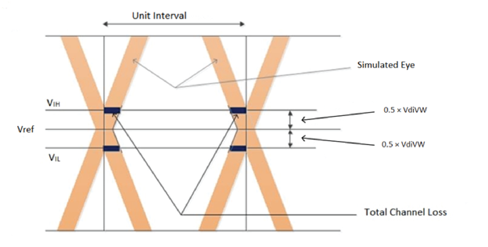
Simulate the write DQ signals and capture eye at the DRAM pins, using DQ Strobe (DQS) as a trigger for the DQ signals of the memory interface simulation. Measure the setup and hold channel losses at the VIH and VIL mentioned in the memory vendor's data sheet
Write Channel Loss = Measured Loss on the Setup side + Measured Loss on the Hold side.
or
Write Channel Loss = UI – (Eye opening at VIH or VIL).
VREF = Voltage level where the eye opening is highest.
VIH = VREF + (0.5 x VdiVW).
VIL = VREF - (0.5 x VdiVW).
Where VdiVW varies by frequency of operation; you can find the VdiVW value in your memory vendor's data sheet.
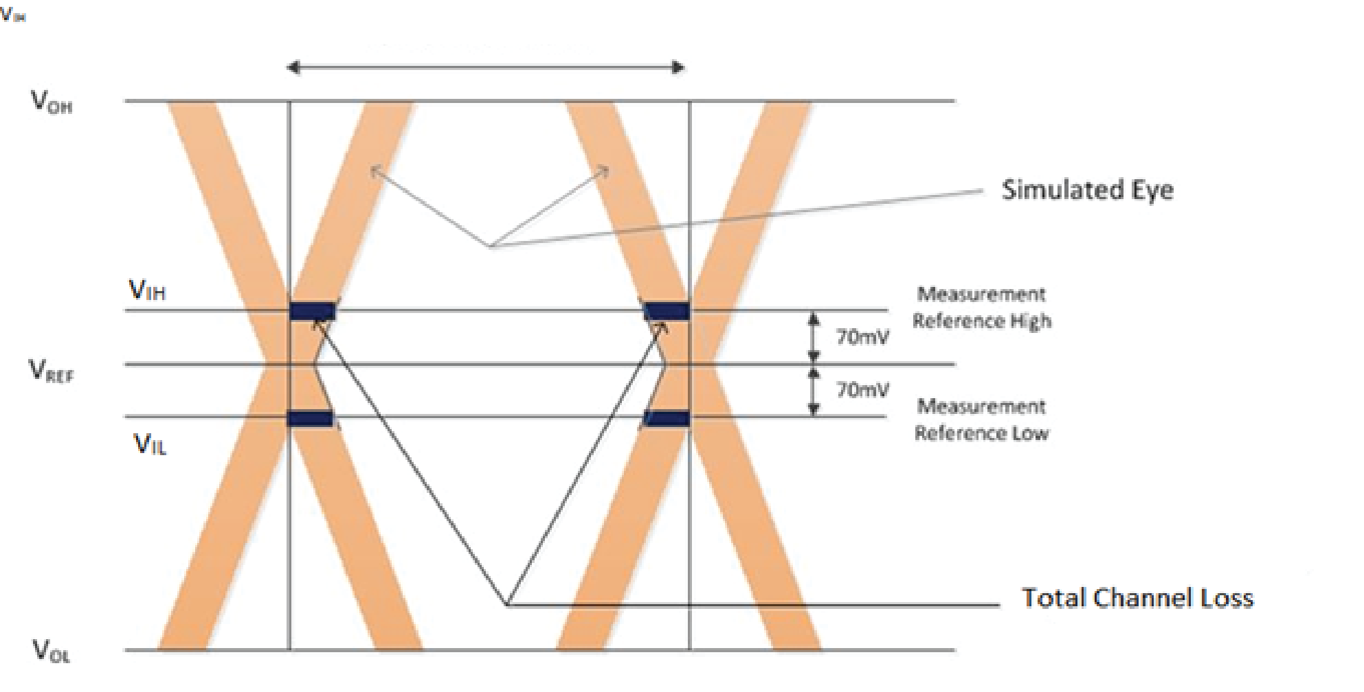
Read DQ ISI and Crosstalk
Simulate read DQ signals and capture eye at the FPGA die. Do not measure at the pin, because you might see unwanted reflections that could create a false representation of the eye opening at the input buffer of the FPGA. Use DQ Strobe (DQS) as a trigger for the DQ signals of your memory interface simulation. Measure the eye opening at +/- 45 mV (VIH/VIL) with respect to VREF.
Read Channel Loss = (UI) - (Eye opening at +/- 45 mV with respect to VREF.)
UI = Unit interval. For example, if you are running your interface at 800 Mhz, the effective data is 1600 Mbps, giving a unit interval of 1/1600 = 625 ps.
VREF = Voltage level where the eye opening is highest.
Write/Read DQS ISI and Crosstalk
Simulate write and read DQS and capture eye. Measure the uncertainty at VREF.
VREF = Voltage level where the eye opening is the highest.