External Memory Interfaces Intel® Stratix® 10 FPGA IP User Guide
A newer version of this document is available. Customers should click here to go to the newest version.
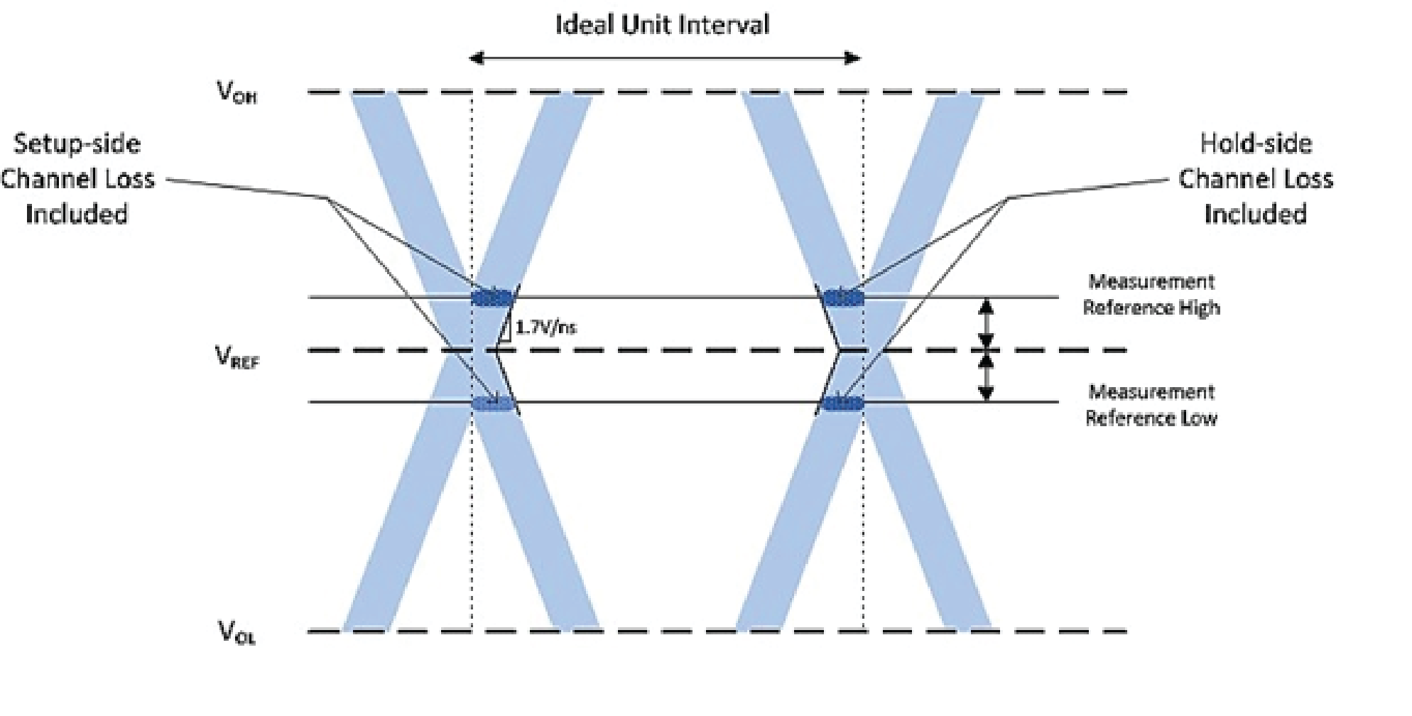
6.5.2.2. Understanding Channel Signal Integrity Measurement
The example below shows a reference eye diagram where the channel loss on the setup- or leading-side of the eye is equal to the channel loss on the hold- or lagging-side of the eye; however, it does not necessarily have to be that way. Because the calibrating PHY calibrates to the center of the read and write eye, the Board Settings tab has parameters for the total extra channel loss for Write DQ and Read DQ. For address and command signals which are not-calibrated, the Board Settings tab allows you to enter setup- and hold-side channel losses that are not equal, allowing the Intel® Quartus® Prime software to place the clock statically within the center of the address and command eye.