External Memory Interfaces Intel® Stratix® 10 FPGA IP User Guide
ID
683741
Date
3/11/2022
Public
A newer version of this document is available. Customers should click here to go to the newest version.
1. Release Information
2. External Memory Interfaces Intel® Stratix® 10 FPGA IP Introduction
3. Intel® Stratix® 10 EMIF IP Product Architecture
4. Intel® Stratix® 10 EMIF IP End-User Signals
5. Intel® Stratix® 10 EMIF – Simulating Memory IP
6. Intel® Stratix® 10 EMIF IP for DDR3
7. Intel® Stratix® 10 EMIF IP for DDR4
8. Intel® Stratix® 10 EMIF IP for QDR II/II+/II+ Xtreme
9. Intel® Stratix® 10 EMIF IP for QDR-IV
10. Intel® Stratix® 10 EMIF IP for RLDRAM 3
11. Intel® Stratix® 10 EMIF IP Timing Closure
12. Optimizing Controller Performance
13. Intel® Stratix® 10 EMIF IP Debugging
14. External Memory Interfaces Intel® Stratix® 10 FPGA IP User Guide Archives
15. Document Revision History for External Memory Interfaces Intel® Stratix® 10 FPGA IP User Guide
3.1. Intel® Stratix® 10 EMIF Architecture: Introduction
3.2. Intel® Stratix® 10 EMIF Sequencer
3.3. Intel® Stratix® 10 EMIF Calibration
3.4. Intel Stratix 10 EMIF IP Controller
3.5. Hardware Resource Sharing Among Multiple Intel® Stratix® 10 EMIFs
3.6. User-requested Reset in Intel® Stratix® 10 EMIF IP
3.7. Intel® Stratix® 10 EMIF for Hard Processor Subsystem
3.8. Intel® Stratix® 10 EMIF Ping Pong PHY
3.1.1. Intel® Stratix® 10 EMIF Architecture: I/O Subsystem
3.1.2. Intel® Stratix® 10 EMIF Architecture: I/O Column
3.1.3. Intel® Stratix® 10 EMIF Architecture: I/O SSM
3.1.4. Intel® Stratix® 10 EMIF Architecture: I/O Bank
3.1.5. Intel® Stratix® 10 EMIF Architecture: I/O Lane
3.1.6. Intel® Stratix® 10 EMIF Architecture: Input DQS Clock Tree
3.1.7. Intel® Stratix® 10 EMIF Architecture: PHY Clock Tree
3.1.8. Intel® Stratix® 10 EMIF Architecture: PLL Reference Clock Networks
3.1.9. Intel® Stratix® 10 EMIF Architecture: Clock Phase Alignment
4.1.1.1. local_reset_req for DDR3
4.1.1.2. local_reset_status for DDR3
4.1.1.3. pll_ref_clk for DDR3
4.1.1.4. pll_locked for DDR3
4.1.1.5. pll_extra_clk_0 for DDR3
4.1.1.6. pll_extra_clk_1 for DDR3
4.1.1.7. pll_extra_clk_2 for DDR3
4.1.1.8. pll_extra_clk_3 for DDR3
4.1.1.9. oct for DDR3
4.1.1.10. mem for DDR3
4.1.1.11. status for DDR3
4.1.1.12. afi_reset_n for DDR3
4.1.1.13. afi_clk for DDR3
4.1.1.14. afi_half_clk for DDR3
4.1.1.15. afi for DDR3
4.1.1.16. emif_usr_reset_n for DDR3
4.1.1.17. emif_usr_clk for DDR3
4.1.1.18. emif_usr_reset_n_sec for DDR3
4.1.1.19. emif_usr_clk_sec for DDR3
4.1.1.20. cal_debug_reset_n for DDR3
4.1.1.21. cal_debug_clk for DDR3
4.1.1.22. cal_debug_out_reset_n for DDR3
4.1.1.23. cal_debug_out_clk for DDR3
4.1.1.24. clks_sharing_master_out for DDR3
4.1.1.25. clks_sharing_slave_in for DDR3
4.1.1.26. clks_sharing_slave_out for DDR3
4.1.1.27. ctrl_amm for DDR3
4.1.1.28. ctrl_auto_precharge for DDR3
4.1.1.29. ctrl_user_priority for DDR3
4.1.1.30. ctrl_ecc_user_interrupt for DDR3
4.1.1.31. ctrl_ecc_readdataerror for DDR3
4.1.1.32. ctrl_ecc_status for DDR3
4.1.1.33. ctrl_mmr_slave for DDR3
4.1.1.34. hps_emif for DDR3
4.1.1.35. cal_debug for DDR3
4.1.1.36. cal_debug_out for DDR3
4.1.2.1. local_reset_req for DDR4
4.1.2.2. local_reset_status for DDR4
4.1.2.3. pll_ref_clk for DDR4
4.1.2.4. pll_locked for DDR4
4.1.2.5. pll_extra_clk_0 for DDR4
4.1.2.6. pll_extra_clk_1 for DDR4
4.1.2.7. pll_extra_clk_2 for DDR4
4.1.2.8. pll_extra_clk_3 for DDR4
4.1.2.9. ac_parity_err for DDR4
4.1.2.10. oct for DDR4
4.1.2.11. mem for DDR4
4.1.2.12. status for DDR4
4.1.2.13. afi_reset_n for DDR4
4.1.2.14. afi_clk for DDR4
4.1.2.15. afi_half_clk for DDR4
4.1.2.16. afi for DDR4
4.1.2.17. emif_usr_reset_n for DDR4
4.1.2.18. emif_usr_clk for DDR4
4.1.2.19. emif_usr_reset_n_sec for DDR4
4.1.2.20. emif_usr_clk_sec for DDR4
4.1.2.21. cal_debug_reset_n for DDR4
4.1.2.22. cal_debug_clk for DDR4
4.1.2.23. cal_debug_out_reset_n for DDR4
4.1.2.24. cal_debug_out_clk for DDR4
4.1.2.25. clks_sharing_master_out for DDR4
4.1.2.26. clks_sharing_slave_in for DDR4
4.1.2.27. clks_sharing_slave_out for DDR4
4.1.2.28. ctrl_amm for DDR4
4.1.2.29. ctrl_auto_precharge for DDR4
4.1.2.30. ctrl_user_priority for DDR4
4.1.2.31. ctrl_ecc_user_interrupt for DDR4
4.1.2.32. ctrl_ecc_readdataerror for DDR4
4.1.2.33. ctrl_ecc_status for DDR4
4.1.2.34. ctrl_mmr_slave for DDR4
4.1.2.35. hps_emif for DDR4
4.1.2.36. cal_debug for DDR4
4.1.2.37. cal_debug_out for DDR4
4.1.3.1. local_reset_req for QDR II/II+/II+ Xtreme
4.1.3.2. local_reset_status for QDR II/II+/II+ Xtreme
4.1.3.3. pll_ref_clk for QDR II/II+/II+ Xtreme
4.1.3.4. pll_locked for QDR II/II+/II+ Xtreme
4.1.3.5. pll_extra_clk_0 for QDR II/II+/II+ Xtreme
4.1.3.6. pll_extra_clk_1 for QDR II/II+/II+ Xtreme
4.1.3.7. pll_extra_clk_2 for QDR II/II+/II+ Xtreme
4.1.3.8. pll_extra_clk_3 for QDR II/II+/II+ Xtreme
4.1.3.9. oct for QDR II/II+/II+ Xtreme
4.1.3.10. mem for QDR II/II+/II+ Xtreme
4.1.3.11. status for QDR II/II+/II+ Xtreme
4.1.3.12. emif_usr_reset_n for QDR II/II+/II+ Xtreme
4.1.3.13. emif_usr_clk for QDR II/II+/II+ Xtreme
4.1.3.14. cal_debug_reset_n for QDR II/II+/II+ Xtreme
4.1.3.15. cal_debug_clk for QDR II/II+/II+ Xtreme
4.1.3.16. cal_debug_out_reset_n for QDR II/II+/II+ Xtreme
4.1.3.17. cal_debug_out_clk for QDR II/II+/II+ Xtreme
4.1.3.18. clks_sharing_master_out for QDR II/II+/II+ Xtreme
4.1.3.19. clks_sharing_slave_in for QDR II/II+/II+ Xtreme
4.1.3.20. clks_sharing_slave_out for QDR II/II+/II+ Xtreme
4.1.3.21. ctrl_amm for QDR II/II+/II+ Xtreme
4.1.3.22. cal_debug for QDR II/II+/II+ Xtreme
4.1.3.23. cal_debug_out for QDR II/II+/II+ Xtreme
4.1.4.1. local_reset_req for QDR-IV
4.1.4.2. local_reset_status for QDR-IV
4.1.4.3. pll_ref_clk for QDR-IV
4.1.4.4. pll_locked for QDR-IV
4.1.4.5. pll_extra_clk_0 for QDR-IV
4.1.4.6. pll_extra_clk_1 for QDR-IV
4.1.4.7. pll_extra_clk_2 for QDR-IV
4.1.4.8. pll_extra_clk_3 for QDR-IV
4.1.4.9. oct for QDR-IV
4.1.4.10. mem for QDR-IV
4.1.4.11. status for QDR-IV
4.1.4.12. afi_reset_n for QDR-IV
4.1.4.13. afi_clk for QDR-IV
4.1.4.14. afi_half_clk for QDR-IV
4.1.4.15. afi for QDR-IV
4.1.4.16. emif_usr_reset_n for QDR-IV
4.1.4.17. emif_usr_clk for QDR-IV
4.1.4.18. cal_debug_reset_n for QDR-IV
4.1.4.19. cal_debug_clk for QDR-IV
4.1.4.20. cal_debug_out_reset_n for QDR-IV
4.1.4.21. cal_debug_out_clk for QDR-IV
4.1.4.22. clks_sharing_master_out for QDR-IV
4.1.4.23. clks_sharing_slave_in for QDR-IV
4.1.4.24. clks_sharing_slave_out for QDR-IV
4.1.4.25. ctrl_amm for QDR-IV
4.1.4.26. cal_debug for QDR-IV
4.1.4.27. cal_debug_out for QDR-IV
4.1.5.1. local_reset_req for RLDRAM 3
4.1.5.2. local_reset_status for RLDRAM 3
4.1.5.3. pll_ref_clk for RLDRAM 3
4.1.5.4. pll_locked for RLDRAM 3
4.1.5.5. pll_extra_clk_0 for RLDRAM 3
4.1.5.6. pll_extra_clk_1 for RLDRAM 3
4.1.5.7. pll_extra_clk_2 for RLDRAM 3
4.1.5.8. pll_extra_clk_3 for RLDRAM 3
4.1.5.9. oct for RLDRAM 3
4.1.5.10. mem for RLDRAM 3
4.1.5.11. status for RLDRAM 3
4.1.5.12. afi_reset_n for RLDRAM 3
4.1.5.13. afi_clk for RLDRAM 3
4.1.5.14. afi_half_clk for RLDRAM 3
4.1.5.15. afi for RLDRAM 3
4.1.5.16. cal_debug_reset_n for RLDRAM 3
4.1.5.17. cal_debug_clk for RLDRAM 3
4.1.5.18. cal_debug_out_reset_n for RLDRAM 3
4.1.5.19. cal_debug_out_clk for RLDRAM 3
4.1.5.20. clks_sharing_master_out for RLDRAM 3
4.1.5.21. clks_sharing_slave_in for RLDRAM 3
4.1.5.22. clks_sharing_slave_out for RLDRAM 3
4.1.5.23. cal_debug for RLDRAM 3
4.1.5.24. cal_debug_out for RLDRAM 3
4.4.1. ctrlcfg0
4.4.2. ctrlcfg1
4.4.3. dramtiming0
4.4.4. caltiming0
4.4.5. caltiming1
4.4.6. caltiming2
4.4.7. caltiming3
4.4.8. caltiming4
4.4.9. caltiming9
4.4.10. dramaddrw
4.4.11. sideband0
4.4.12. sideband1
4.4.13. sideband4
4.4.14. sideband6
4.4.15. sideband7
4.4.16. sideband9
4.4.17. sideband11
4.4.18. sideband12
4.4.19. sideband13
4.4.20. sideband14
4.4.21. dramsts
4.4.22. niosreserve0
4.4.23. niosreserve1
4.4.24. sideband16
4.4.25. ecc3: ECC Error and Interrupt Configuration
4.4.26. ecc4: Status and Error Information
4.4.27. ecc5: Address of Most Recent SBE/DBE
4.4.28. ecc6: Address of Most Recent Correction Command Dropped
4.4.29. ecc7: Extension for Address of Most Recent SBE/DBE
4.4.30. ecc8: Extension for Address of Most Recent Correction Command Dropped
6.1.1. Intel Stratix 10 EMIF IP DDR3 Parameters: General
6.1.2. Intel Stratix 10 EMIF IP DDR3 Parameters: FPGA I/O
6.1.3. Intel Stratix 10 EMIF IP DDR3 Parameters: Memory
6.1.4. Intel Stratix 10 EMIF IP DDR3 Parameters: Mem I/O
6.1.5. Intel Stratix 10 EMIF IP DDR3 Parameters: Mem Timing
6.1.6. Intel Stratix 10 EMIF IP DDR3 Parameters: Board
6.1.7. Intel Stratix 10 EMIF IP DDR3 Parameters: Controller
6.1.8. Intel Stratix 10 EMIF IP DDR3 Parameters: Diagnostics
6.1.9. Intel Stratix 10 EMIF IP DDR3 Parameters: Example Designs
7.1.1. Intel Stratix 10 EMIF IP DDR4 Parameters: General
7.1.2. Intel Stratix 10 EMIF IP DDR4 Parameters: FPGA I/O
7.1.3. Intel Stratix 10 EMIF IP DDR4 Parameters: Memory
7.1.4. Intel Stratix 10 EMIF IP DDR4 Parameters: Mem I/O
7.1.5. Intel Stratix 10 EMIF IP DDR4 Parameters: Mem Timing
7.1.6. Intel Stratix 10 EMIF IP DDR4 Parameters: Board
7.1.7. Intel Stratix 10 EMIF IP DDR4 Parameters: Controller
7.1.8. Intel Stratix 10 EMIF IP DDR4 Parameters: Diagnostics
7.1.9. Intel Stratix 10 EMIF IP DDR4 Parameters: Example Designs
7.5.4.1. General Layout Guidelines
7.5.4.2. Layout Guidelines
7.5.4.3. Length Matching Rules
7.5.4.4. Spacing Guidelines
7.5.4.5. Layout Guidelines for DDR3 and DDR4 SDRAM Wide Interface (>72 bits)
7.5.4.6. Fly-By Network Design for Clock, Command, and Address Signals
7.5.4.7. Clamshell Topology
7.5.4.8. Additional Layout Guidelines for DDR4 Twin-die Devices
8.1.1. Intel Stratix 10 EMIF IP QDR II/II+/II+ Xtreme Parameters: General
8.1.2. Intel Stratix 10 EMIF IP QDR II/II+/II+ Xtreme Parameters: FPGA I/O
8.1.3. Intel Stratix 10 EMIF IP QDR II/II+/II+ Xtreme Parameters: Memory
8.1.4. Intel Stratix 10 EMIF IP QDR II/II+/II+ Xtreme Parameters: Mem Timing
8.1.5. Intel Stratix 10 EMIF IP QDR II/II+/II+ Xtreme Parameters: Board
8.1.6. Intel Stratix 10 EMIF IP QDR II/II+/II+ Xtreme Parameters: Controller
8.1.7. Intel Stratix 10 EMIF IP QDR II/II+/II+ Xtreme Parameters: Diagnostics
8.1.8. Intel Stratix 10 EMIF IP QDR II/II+/II+ Xtreme Parameters: Example Designs
8.3.1.6.1. General Guidelines
8.3.1.6.2. QDR II, QDR II+ and QDR II+ Xtreme SRAM Command Signals
8.3.1.6.3. QDR II, QDR II+ and QDR II+ Xtreme SRAM Address Signals
8.3.1.6.4. QDR II, QDR II+, and QDR II+ Xtreme SRAM Clock Signals
8.3.1.6.5. QDR II, QDR II+ and QDR II+ Xtreme SRAM Data, BWS, and QVLD Signals
8.3.1.6.6. Resource Sharing Guidelines (Multiple Interfaces)
9.1.1. Intel Stratix 10 EMIF IP QDR-IV Parameters: General
9.1.2. Intel Stratix 10 EMIF IP QDR-IV Parameters: FPGA I/O
9.1.3. Intel Stratix 10 EMIF IP QDR-IV Parameters: Memory
9.1.4. Intel Stratix 10 EMIF IP QDR-IV Parameters: Mem Timing
9.1.5. Intel Stratix 10 EMIF IP QDR-IV Parameters: Board
9.1.6. Intel Stratix 10 EMIF IP QDR-IV Parameters: Controller
9.1.7. Intel Stratix 10 EMIF IP QDR-IV Parameters: Diagnostics
9.1.8. Intel Stratix 10 EMIF IP QDR-IV Parameters: Example Designs
10.1.1. Intel Stratix 10 EMIF IP RLDRAM 3 Parameters: General
10.1.2. Intel Stratix 10 EMIF IP RLDRAM 3 Parameters: FPGA I/O
10.1.3. Intel Stratix 10 EMIF IP RLDRAM 3 Parameters: Memory
10.1.4. Intel Stratix 10 EMIF IP RLDRAM 3 Parameters: Mem Timing
10.1.5. Intel Stratix 10 EMIF IP RLDRAM 3 Parameters: Board
10.1.6. Intel Stratix 10 EMIF IP RLDRAM 3 Parameters: Diagnostics
10.1.7. Intel Stratix 10 EMIF IP RLDRAM 3 Parameters: Example Designs
12.4.1. Auto-Precharge Commands
12.4.2. Latency
12.4.3. Calibration
12.4.4. Bank Interleaving
12.4.5. Additive Latency and Bank Interleaving
12.4.6. User-Controlled Refresh
12.4.7. Frequency of Operation
12.4.8. Series of Reads or Writes
12.4.9. Data Reordering
12.4.10. Starvation Control
12.4.11. Command Reordering
12.4.12. Bandwidth
12.4.13. Enable Command Priority Control
13.1. Interface Configuration Performance Issues
13.2. Functional Issue Evaluation
13.3. Timing Issue Characteristics
13.4. Verifying Memory IP Using the Signal Tap II Logic Analyzer
13.5. Hardware Debugging Guidelines
13.6. Categorizing Hardware Issues
13.7. Debugging Intel® Stratix® 10 EMIF IP
13.8. Using the Default Traffic Generator
13.9. Using the Configurable Traffic Generator (TG2)
13.5.1. Create a Simplified Design that Demonstrates the Same Issue
13.5.2. Measure Power Distribution Network
13.5.3. Measure Signal Integrity and Setup and Hold Margin
13.5.4. Vary Voltage
13.5.5. Operate at a Lower Speed
13.5.6. Determine Whether the Issue Exists in Previous Versions of Software
13.5.7. Determine Whether the Issue Exists in the Current Version of Software
13.5.8. Try A Different PCB
13.5.9. Try Other Configurations
13.5.10. Debugging Checklist
13.7.1. Debugging With the Legacy External Memory Interface Debug Toolkit
13.7.2. Debugging with the External Memory Interface Unified Calibration Debug Toolkit
13.7.3. On-Chip Debug Port for Intel® Stratix® 10 EMIF IP
13.7.4. Legacy Efficiency Monitor and Protocol Checker
13.7.5. New Efficiency Monitor
13.7.1.1. User Interface
13.7.1.2. Communication
13.7.1.3. Setup and Use
13.7.1.4. Configuring Your EMIF IP for Use with the Legacy Debug Toolkit
13.7.1.5. Reports
13.7.1.6. On-Die Termination Calibration
13.7.1.7. Eye Diagram
13.7.1.8. Driver Margining for Intel® Stratix® 10 EMIF IP
13.7.1.9. Example Tcl Script for Running the Legacy EMIF Debug Toolkit
13.7.1.10. Using the Legacy EMIF Debug Toolkit with Intel® Stratix® 10 HPS Interfaces
13.7.2.1. Prerequisites for Using the EMIF Unified Calibration Debug Toolkit
13.7.2.2. Configuring a Design to use the EMIF Unified Calibration Debug Toolkit
13.7.2.3. Launching the EMIF Debug Toolkit
13.7.2.4. Using the EMIF Debug Toolkit
13.7.2.5. Exporting Tables
13.7.2.6. Viewing Diagrams in the Eye Viewer
13.7.2.7. Guidelines for Debugging Calibration Issues
13.7.2.7.1. Debugging Calibration Failure Using Information from the Calibration report
13.7.2.7.2. Debugging Address and Command Leveling Calibration Failure
13.7.2.7.3. Debugging Address and Command Deskew Failure
13.7.2.7.4. Debugging DQS Enable Failure
13.7.2.7.5. Debugging Read Deskew Calibration Failure
13.7.2.7.6. Debugging VREFIN Calibration Failure
13.7.2.7.7. Debugging LFIFO Calibration Failure
13.7.2.7.8. Debugging Write Leveling Failure
13.7.2.7.9. Debugging Write Deskew Calibration Failure
13.7.2.7.10. Debugging VREFOUT Calibration Failure
13.9.1. Enabling the Traffic Generator in a Design Example
13.9.2. Traffic Generator Block Description
13.9.3. Default Traffic Pattern
13.9.4. Configuration and Status Registers
13.9.5. User Pattern
13.9.6. Traffic Generator Status
13.9.7. Starting Traffic with the Traffic Generator
13.9.8. Traffic Generator Configuration User Interface
13.9.9. Examples of Configuring the TG2 Traffic Generator
Example 1: Configuring TG2 to Write and Read from All Memory Locations with Alternating 0x555_5555_5555_5555 and 0xAAA_AAAA_AAAA_AAAA Data Pattern
Example 2: Configuring TG2 to Run with an Infinite Loop
13.9.9. Examples of Configuring the TG2 Traffic Generator
Example 1: Configuring TG2 to Write and Read from All Memory Locations with Alternating 0x555_5555_5555_5555 and 0xAAA_AAAA_AAAA_AAAA Data Pattern
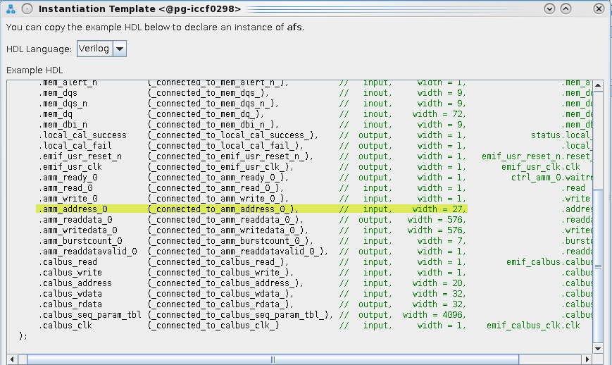
In this example, 227 logical addresses are available on the EMIF controller. This example is a x72 DDR4 interface, configured to use Quarter Rate (QR) user logic.
Figure 208. Address Width for Memory IP
To write to all memory locations for a memory IP, starting from address=0x0 , it is necessary to satisfy the following requirement:
TG_LOOP_COUNT x TG_BURST_LENGTH x TG_WRITE_COUNT = Total Logical Address AvailableFor this example, assume the following:
- TG_BURST_LENGTH = 64 (in decimal) or TG_BURST_LENGTH = 0x40 (in hexadecimal).
- TG_WRITE_COUNT = 1.
You can calculate the required TG_LOOP_COUNT as follows:
TG_LOOP_COUNT = Total Logical Address Available / (TG_WRITE_COUNT x TG_BURST_LENGTH)
= 227/64
= 2097152 (in decimal)
= 0x20_0000 (in hexadecimal)
To configure the TG2 using core logic, follow these steps:
- Write to TG_CLEAR with data=0xF to clear all the failure status registers.
- Configure the registers with the value specified in table 1 below.
- Write to TG_START to start the TG2 using the configuration in step 2. This starts the traffic test in user mode.
- Read from TG_TEST_COMPLETE until the read data =0x1, indicating the traffic test has completed.
- Read from TG_PASS, TG_FAIL, and TG_TIMEOUT to check the test result.
- TG_PASS. A value of 1 indicates that the traffic test passed at the end of all test stages.
- TG_FAIL. A value of 1 indicates that the configured traffic finished running but a failure (read miscompare) was observed. You may read from other relevant registers to get more information about the failure. Refer to the Configuration and Status Registers table for information on the available registers.
- TG_TIMEOUT. A value of 1 indicates that a read response was not received from the interface for one or more read commands.
| Address | Register Name | Value | Remarks |
|---|---|---|---|
| 0x8 | TG_LOOP_COUNT | 0x20_0000 | Require 2097152* 64 to cover all memory locations. |
| 0xC | TG_WRITE_COUNT | 0x1 | |
| 0x10 | TG_READ_COUNT | 0x1 | |
| 0x14 | TG_WRITE_REPEAT_COUNT | 0x1 | |
| 0x18 | TG_READ_REPEAT_COUNT | 0x1 | |
| 0x1C | TG_BURST_LENGTH | 0x40 | Require 2097152* 64 to cover all memory locations. |
| 0x38 | TG_RW_GEN_IDLE_COUNT | 0x1 | |
| 0x3C | TG_RW_GEN_LOOP_IDLE_COUNT | 0x1 | |
| 0x40 | TG_SEQ_START_ADDR_WR_L | 0x0 | Lower 32-bit of start write address. |
| 0x44 | TG_SEQ_START_ADDR_WR_H | 0x0 | Upper 32-bit of start write address. |
| 0x48 | TG_ADDR_MODE_WR | 0x1 | Sequential Addressing. |
| 0x50 | TG_RETURN_TO_START_ADDR | 0x0 | |
| 0x74 | TG_SEQ_ADDR_INCR | 0x40 | Must match the burst length in this example. |
| 0x78 | TG_SEQ_START_ADDR_RD_L | 0x0 | Lower 32-bit of start read address. |
| 0x7C | TG_SEQ_START_ADDR_RD_H | 0x0 | Upper 32-bit of start read address. |
| 0x80 | TG_ADDR_MODE_RD | 0x1 | Sequential Addressing. Must match the TG_ADDR_MODE_WR. |
| 0xB4 | TG_USER_WORM_EN | 0x0 | Disable WORM mode. |
| 0xE80 | TG_BYTEEN_SEL | 0x0 | Fixed Pattern. |
| 0xC00 | TG_PPPG_SEL | 0x0 | Fixed Pattern. |
| 0x400 | TG_DATA_SEED | 0x5555_5555 | For DG0 (DQ0/8/16/24/32/40/48/56/64). |
| 0x404 | TG_DATA_SEED | 0xAAAA_AAAA | For DG1 (DQ1/9/17/25/33/41/49/57/65). |
| 0x408 | TG_DATA_SEED | 0x5555_5555 | For DG2 (DQ2/10/18/26/34/42/50/58/66). |
| 0x40C | TG_DATA_SEED | 0xAAAA_AAAA | For DG3 (DQ3/11/19/27/35/43/51/59/67). |
| 0x410 | TG_DATA_SEED | 0x5555_5555 | For DG4 (DQ4/12/20/28/36/44/52/60/68). |
| 0x414 | TG_DATA_SEED | 0xAAAA_AAAA | For DG5 (DQ5/13/21/29/37/45/53/61/69). |
| 0x418 | TG_DATA_SEED | 0x5555_5555 | For DG6 (DQ6/14/22/20/38/46/54/62/70). |
| 0x41C | TG_DATA_SEED | 0xAAAA_AAAA | For DG7 (DQ7/15/23/31/39/47/55/63/71). |
| 0x800 | TG_BYTEEN_SEED | 0xFFFF_FFFF | For Byte 0. |
| 0x804 | TG_BYTEEN_SEED | 0xFFFF_FFFF | For Byte 1. |
| 0x808 | TG_BYTEEN_SEED | 0xFFFF_FFFF | For Byte 2. |
| 0x80C | TG_BYTEEN_SEED | 0xFFFF_FFFF | For Byte 3. |
| 0x810 | TG_BYTEEN_SEED | 0xFFFF_FFFF | For Byte 4. |
| 0x814 | TG_BYTEEN_SEED | 0xFFFF_FFFF | For Byte 5. |
| 0x818 | TG_BYTEEN_SEED | 0xFFFF_FFFF | For Byte 6. |
| 0x81C | TG_BYTEEN_SEED | 0xFFFF_FFFF | For Byte 7. |
| 0x820 | TG_BYTEEN_SEED | 0xFFFF_FFFF | For Byte 8. |
Example 2: Configuring TG2 to Run with an Infinite Loop
- Clear all the failure status registers. Write to TG_CLEAR with data=0xF.
- Configure the TG2 with the access and data pattern you want.
- Write to TG_LOOP_COUNT with data=0x0.
- Write to TG_START with a 0 or 1 to start TG2.
- To stop the TG2 while running an infinite loop, write to TG_LOOP_COUNT with data=0x1.