Arria® 10 Hard Processor System Technical Reference Manual
29.1.3. FPGA-to-HPS SDRAM Interface
The FPGA-to-HPS SDRAM interface is a direct connection between the FPGA fabric and the HPS SDRAM controller. The interface is highly configurable, allowing a mix between the four port configurations and the port width. The FPGA-to-HPS SDRAM interface supports AMBA* AXI* interface standards.
| Interface Name | Associated Data Interface | Associated Clock Interface |
|---|---|---|
| F2SDRAM0 | f2sdram0_data | f2sdram0_clock |
| F2SDRAM1 | f2sdram1_data | f2sdram1_clock |
| F2SDRAM2 | f2sdram2_data | f2sdram2_clcok |
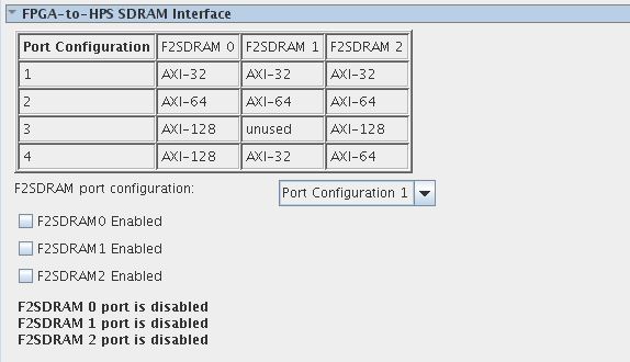
The FPGA-to-HPS SDRAM interface is a configurable interface to the multi-port SDRAM controller. There are four port configurations that are a combination of the SDRAM ports 0 - 2 that you are able to select. Once a port configuration is selected, you can choose to enable the ports that you need.
The total data width of all interfaces is limited to a maximum of 256 bits in the read direction and 256 bits in the write direction. The HPS SDRAM controller supports up to 3 masters (command ports), 3x 64-bit read data ports and 3x 64-bit write data ports.