External Memory Interface Handbook Volume 3: Reference Material: For UniPHY-based Device Families
ID
683841
Date
3/06/2023
Public
1. Functional Description—UniPHY
2. Functional Description— Intel® MAX® 10 EMIF IP
3. Functional Description—Hard Memory Interface
4. Functional Description—HPS Memory Controller
5. Functional Description—HPC II Controller
6. Functional Description—QDR II Controller
7. Functional Description—RLDRAM II Controller
8. Functional Description—RLDRAM 3 PHY-Only IP
9. Functional Description—Example Designs
10. Introduction to UniPHY IP
11. Latency for UniPHY IP
12. Timing Diagrams for UniPHY IP
13. External Memory Interface Debug Toolkit
14. Upgrading to UniPHY-based Controllers from ALTMEMPHY-based Controllers
1.1. I/O Pads
1.2. Reset and Clock Generation
1.3. Dedicated Clock Networks
1.4. Address and Command Datapath
1.5. Write Datapath
1.6. Read Datapath
1.7. Sequencer
1.8. Shadow Registers
1.9. UniPHY Interfaces
1.10. UniPHY Signals
1.11. PHY-to-Controller Interfaces
1.12. Using a Custom Controller
1.13. AFI 3.0 Specification
1.14. Register Maps
1.15. Ping Pong PHY
1.16. Efficiency Monitor and Protocol Checker
1.17. UniPHY Calibration Stages
1.18. Document Revision History
1.7.1.1. Nios® II-based Sequencer Function
1.7.1.2. Nios® II-based Sequencer Architecture
1.7.1.3. Nios® II-based Sequencer SCC Manager
1.7.1.4. Nios® II-based Sequencer RW Manager
1.7.1.5. Nios® II-based Sequencer PHY Manager
1.7.1.6. Nios® II-based Sequencer Data Manager
1.7.1.7. Nios® II-based Sequencer Tracking Manager
1.7.1.8. Nios® II-based Sequencer Processor
1.7.1.9. Nios® II-based Sequencer Calibration and Diagnostics
1.17.1. Calibration Overview
1.17.2. Calibration Stages
1.17.3. Memory Initialization
1.17.4. Stage 1: Read Calibration Part One—DQS Enable Calibration and DQ/DQS Centering
1.17.5. Stage 2: Write Calibration Part One
1.17.6. Stage 3: Write Calibration Part Two—DQ/DQS Centering
1.17.7. Stage 4: Read Calibration Part Two—Read Latency Minimization
1.17.8. Calibration Signals
1.17.9. Calibration Time
4.1. Features of the SDRAM Controller Subsystem
4.2. SDRAM Controller Subsystem Block Diagram
4.3. SDRAM Controller Memory Options
4.4. SDRAM Controller Subsystem Interfaces
4.5. Memory Controller Architecture
4.6. Functional Description of the SDRAM Controller Subsystem
4.7. SDRAM Power Management
4.8. DDR PHY
4.9. Clocks
4.10. Resets
4.11. Port Mappings
4.12. Initialization
4.13. SDRAM Controller Subsystem Programming Model
4.14. Debugging HPS SDRAM in the Preloader
4.15. SDRAM Controller Address Map and Register Definitions
4.16. Document Revision History
10.7.1. DDR2, DDR3, and LPDDR2 Resource Utilization in Arria V Devices
10.7.2. DDR2 and DDR3 Resource Utilization in Arria II GZ Devices
10.7.3. DDR2 and DDR3 Resource Utilization in Stratix III Devices
10.7.4. DDR2 and DDR3 Resource Utilization in Stratix IV Devices
10.7.5. DDR2 and DDR3 Resource Utilization in Arria V GZ and Stratix V Devices
10.7.6. QDR II and QDR II+ Resource Utilization in Arria V Devices
10.7.7. QDR II and QDR II+ Resource Utilization in Arria II GX Devices
10.7.8. QDR II and QDR II+ Resource Utilization in Arria II GZ, Arria V GZ, Stratix III, Stratix IV, and Stratix V Devices
10.7.9. RLDRAM II Resource Utilization in Arria® V Devices
10.7.10. RLDRAM II Resource Utilization in Arria® II GZ, Arria® V GZ, Stratix® III, Stratix® IV, and Stratix® V Devices
13.1. User Interface
13.2. Setup and Use
13.3. Operational Considerations
13.4. Troubleshooting
13.5. Debug Report for Arria V and Cyclone V SoC Devices
13.6. On-Chip Debug Port for UniPHY-based EMIF IP
13.7. Example Tcl Script for Running the Legacy EMIF Debug Toolkit
13.8. Document Revision History
12.2. DDR3 Timing Diagrams
This topic contains timing diagrams for UniPHY-based external memory interface IP for DDR3 protocols.
The following figures present timing diagrams based on a Stratix III device
Figure 75. Half-Rate DDR3 SDRAM Read
Notes for the above Figure:
- Controller receives read command.
- Controller issues activate command to PHY.
- PHY issues activate command to memory.
- Controller issues read command to PHY.
- PHY issues read command to memory.
- PHY receives read data from memory.
- Controller receives read data from PHY.
- User logic receives read data from controller.
Figure 76. Half-Rate DDR3 SDRAM Writes
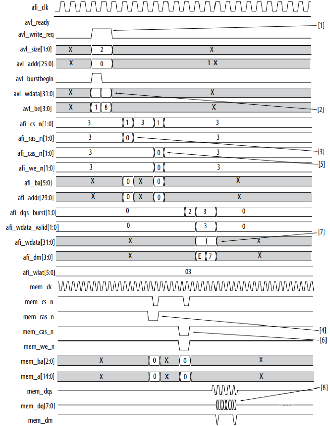
Notes for the above Figure:
- Controller receives write command.
- Controller receives write data.
- Controller issues activate command to PHY.
- PHY issues activate command to memory.
- Controller issues write command to PHY.
- PHY issues write command to memory.
- Controller sends write data to PHY.
- PHY sends write data to memory.
Figure 77. Quarter-Rate DDR3 SDRAM Reads
Notes for the above Figure:
- Controller receives read command.
- Controller issues activate command to PHY.
- PHY issues activate command to memory.
- Controller issues read command to PHY.
- PHY issues read command to memory.
- PHY receives read data from memory
- Controller receives read data from PHY
- User logic receives read data from controller.
Figure 78. Quarter-Rate DDR3 SDRAM Writes
Notes for the above Figure:
- Controller receives write command.
- Controller receives write data.
- Controller issues activate command to PHY
- PHY issues activate command to memory.
- Controller issues write command to PHY
- PHY issues write command to memory
- Controller sends write data to PHY
- PHY sends write data to memory.