Visible to Intel only — GUID: bos1493517947427
Ixiasoft
1. Functional Description—UniPHY
2. Functional Description— Intel® Stratix® 10 EMIF IP
3. Functional Description— Intel® Arria® 10 EMIF IP
4. Functional Description— Intel® MAX® 10 EMIF IP
5. Functional Description—Hard Memory Interface
6. Functional Description—HPS Memory Controller
7. Functional Description—HPC II Controller
8. Functional Description—QDR II Controller
9. Functional Description—QDR-IV Controller
10. Functional Description—RLDRAM II Controller
11. Functional Description—RLDRAM 3 PHY-Only IP
12. Functional Description—Example Designs
13. Introduction to UniPHY IP
14. Latency for UniPHY IP
15. Timing Diagrams for UniPHY IP
16. External Memory Interface Debug Toolkit
17. Upgrading to UniPHY-based Controllers from ALTMEMPHY-based Controllers
1.1. I/O Pads
1.2. Reset and Clock Generation
1.3. Dedicated Clock Networks
1.4. Address and Command Datapath
1.5. Write Datapath
1.6. Read Datapath
1.7. Sequencer
1.8. Shadow Registers
1.9. UniPHY Interfaces
1.10. UniPHY Signals
1.11. PHY-to-Controller Interfaces
1.12. Using a Custom Controller
1.13. AFI 3.0 Specification
1.14. Register Maps
1.15. Ping Pong PHY
1.16. Efficiency Monitor and Protocol Checker
1.17. UniPHY Calibration Stages
1.18. Document Revision History
1.7.1.1. NIOS II-based Sequencer Function
1.7.1.2. Nios II-based Sequencer Architecture
1.7.1.3. Nios II-based Sequencer SCC Manager
1.7.1.4. NIOS II-based Sequencer RW Manager
1.7.1.5. NIOS II-based Sequencer PHY Manager
1.7.1.6. NIOS II-based Sequencer Data Manager
1.7.1.7. NIOS II-based Sequencer Tracking Manager
1.7.1.8. NIOS II-based Sequencer Processor
1.7.1.9. NIOS II-based Sequencer Calibration and Diagnostics
1.17.1. Calibration Overview
1.17.2. Calibration Stages
1.17.3. Memory Initialization
1.17.4. Stage 1: Read Calibration Part One—DQS Enable Calibration and DQ/DQS Centering
1.17.5. Stage 2: Write Calibration Part One
1.17.6. Stage 3: Write Calibration Part Two—DQ/DQS Centering
1.17.7. Stage 4: Read Calibration Part Two—Read Latency Minimization
1.17.8. Calibration Signals
1.17.9. Calibration Time
2.1. Stratix® 10 Supported Memory Protocols
2.2. Stratix® 10 EMIF IP Support for 3DS/TSV DDR4 Devices
2.3. Migrating to Stratix® 10 from Previous Device Families
2.4. Stratix® 10 EMIF Architecture: Introduction
2.5. Hardware Resource Sharing Among Multiple Stratix® 10 EMIFs
2.6. Stratix® 10 EMIF IP Component
2.7. Examples of External Memory Interface Implementations for DDR4
2.8. Stratix® 10 EMIF Sequencer
2.9. Stratix® 10 EMIF Calibration
2.10. Stratix 10 EMIF and SmartVID
2.11. Stratix® 10 Hard Memory Controller Rate Conversion Feature
2.12. Differences Between User-Requested Reset in Stratix® 10 versus Arria® 10
2.13. Compiling Stratix® 10 EMIF IP with the Quartus Prime Software
2.14. Debugging Stratix® 10 EMIF IP
2.15. Stratix® 10 EMIF for Hard Processor Subsystem
2.16. Stratix® 10 EMIF Ping Pong PHY
2.17. AFI 4.0 Specification
2.18. Stratix® 10 Resource Utilization
2.19. Stratix® 10 EMIF Latency
2.20. Integrating a Custom Controller with the Hard PHY
2.21. Document Revision History
2.4.1. Stratix® 10 EMIF Architecture: I/O Subsystem
2.4.2. Stratix® 10 EMIF Architecture: I/O Column
2.4.3. Stratix® 10 EMIF Architecture: I/O SSM
2.4.4. Stratix® 10 EMIF Architecture: I/O Bank
2.4.5. Stratix® 10 EMIF Architecture: I/O Lane
2.4.6. Stratix® 10 EMIF Architecture: Input DQS Clock Tree
2.4.7. Stratix® 10 EMIF Architecture: PHY Clock Tree
2.4.8. Stratix® 10 EMIF Architecture: PLL Reference Clock Networks
2.4.9. Stratix® 10 EMIF Architecture: Clock Phase Alignment
3.1. Supported Memory Protocols
3.2. Key Differences Compared to UniPHY IP and Previous Device Families
3.3. Migrating from Previous Device Families
3.4. Arria® 10 EMIF Architecture: Introduction
3.5. Hardware Resource Sharing Among Multiple EMIFs
3.6. Arria® 10 EMIF IP Component
3.7. Examples of External Memory Interface Implementations for DDR4
3.8. Arria® 10 EMIF Sequencer
3.9. Arria® 10 EMIF Calibration
3.10. Back-to-Back User-Controlled Refresh Usage in Arria® 10
3.11. Arria® 10 EMIF and SmartVID
3.12. Hard Memory Controller Rate Conversion Feature
3.13. Back-to-Back User-Controlled Refresh for Hard Memory Controller
3.14. Compiling Arria® 10 EMIF IP with the Quartus Prime Software
3.15. Debugging Arria® 10 EMIF IP
3.16. Arria® 10 EMIF for Hard Processor Subsystem
3.17. Arria® 10 EMIF Ping Pong PHY
3.18. AFI 4.0 Specification
3.19. Resource Utilization
3.20. Arria® 10 EMIF Latency
3.21. Arria® 10 EMIF Calibration Times
3.22. Integrating a Custom Controller with the Hard PHY
3.23. Memory Mapped Register (MMR) Tables
3.247.7. Document Revision History3.247.7. Document Revision History
3.4.1. Arria® 10 EMIF Architecture: I/O Subsystem
3.4.2. Arria® 10 EMIF Architecture: I/O Column
3.4.3. Arria® 10 EMIF Architecture: I/O AUX
3.4.4. Arria® 10 EMIF Architecture: I/O Bank
3.4.5. Arria® 10 EMIF Architecture: I/O Lane
3.4.6. Arria® 10 EMIF Architecture: Input DQS Clock Tree
3.4.7. Arria® 10 EMIF Architecture: PHY Clock Tree
3.4.8. Arria® 10 EMIF Architecture: PLL Reference Clock Networks
3.4.9. Arria® 10 EMIF Architecture: Clock Phase Alignment
3.23.1. ctrlcfg0: Controller Configuration
3.23.2. ctrlcfg1: Controller Configuration
3.23.3. ctrlcfg2: Controller Configuration
3.23.4. ctrlcfg3: Controller Configuration
3.23.5. ctrlcfg4: Controller Configuration
3.23.6. ctrlcfg5: Controller Configuration
3.23.7. ctrlcfg6: Controller Configuration
3.23.8. ctrlcfg7: Controller Configuration
3.23.9. ctrlcfg8: Controller Configuration
3.23.10. ctrlcfg9: Controller Configuration
3.23.11. dramtiming0: Timing Parameters
3.23.12. dramodt0: On-Die Termination Parameters
3.23.13. dramodt1: On-Die Termination Parameters
3.23.14. sbcfg0: Sideband Configuration
3.23.15. sbcfg1: Sideband Configuration
3.23.16. sbcfg2: Sideband Configuration
3.23.17. sbcfg3: Sideband Configuration
3.23.18. sbcfg4: Sideband Configuration
3.23.19. sbcfg5: Sideband Configuration
3.23.20. sbcfg6: Sideband Configuration
3.23.21. sbcfg7: Sideband Configuration
3.23.22. sbcfg8: Sideband Configuration
3.23.23. sbcfg9: Sideband Configuration
3.23.24. caltiming0: Command/Address/Latency Parameters
3.23.25. caltiming1: Command/Address/Latency Parameters
3.23.26. caltiming2: Command/Address/Latency Parameters
3.23.27. caltiming3: Command/Address/Latency Parameters
3.23.28. caltiming4: Command/Address/Latency Parameters
3.23.29. caltiming5: Command/Address/Latency Parameters
3.23.30. caltiming6: Command/Address/Latency Parameters
3.23.31. caltiming7: Command/Address/Latency Parameters
3.23.32. caltiming8: Command/Address/Latency Parameters
3.23.33. caltiming9: Command/Address/Latency Parameters
3.23.34. caltiming10: Command/Address/Latency Parameters
3.23.35. dramaddrw: Row/Column/Bank Address Width Configuration
3.23.36. sideband0: Sideband
3.23.37. sideband1: Sideband
3.23.38. sideband2: Sideband
3.23.39. sideband3: Sideband
3.23.40. sideband4: Sideband
3.23.41. sideband5: Sideband
3.23.42. sideband6: Sideband
3.23.43. sideband7: Sideband
3.23.44. sideband8: Sideband
3.23.45. sideband9: Sideband
3.23.46. sideband10: Sideband
3.23.47. sideband11: Sideband
3.23.48. sideband12: Sideband
3.23.49. sideband13: Sideband
3.23.50. sideband14: Sideband
3.23.51. sideband15: Sideband
3.23.52. dramsts: Calibration Status
3.23.53. ecc1: ECC General Configuration
3.23.54. ecc2: Width Configuration
3.23.55. ecc3: ECC Error and Interrupt Configuration
3.23.56. ecc4: Status and Error Information
3.23.57. ecc5: Address of Most Recent SBE/DBE
3.23.58. ecc6: Address of Most Recent Correct Command Dropped
6.1. Features of the SDRAM Controller Subsystem
6.2. SDRAM Controller Subsystem Block Diagram
6.3. SDRAM Controller Memory Options
6.4. SDRAM Controller Subsystem Interfaces
6.5. Memory Controller Architecture
6.6. Functional Description of the SDRAM Controller Subsystem
6.7. SDRAM Power Management
6.8. DDR PHY
6.9. Clocks
6.10. Resets
6.11. Port Mappings
6.12. Initialization
6.13. SDRAM Controller Subsystem Programming Model
6.14. Debugging HPS SDRAM in the Preloader
6.15. SDRAM Controller Address Map and Register Definitions
6.16. Document Revision History
13.7.1. DDR2, DDR3, and LPDDR2 Resource Utilization in Arria V Devices
13.7.2. DDR2 and DDR3 Resource Utilization in Arria II GZ Devices
13.7.3. DDR2 and DDR3 Resource Utilization in Stratix III Devices
13.7.4. DDR2 and DDR3 Resource Utilization in Stratix IV Devices
13.7.5. DDR2 and DDR3 Resource Utilization in Arria V GZ and Stratix V Devices
13.7.6. QDR II and QDR II+ Resource Utilization in Arria V Devices
13.7.7. QDR II and QDR II+ Resource Utilization in Arria II GX Devices
13.7.8. QDR II and QDR II+ Resource Utilization in Arria II GZ, Arria V GZ, Stratix III, Stratix IV, and Stratix V Devices
13.7.9. RLDRAM II Resource Utilization in Arria V Devices
13.7.10. RLDRAM II Resource Utilization in Arria II GZ, Arria V GZ, Stratix III, Stratix IV, and Stratix V Devices
16.1. User Interface
16.2. Setup and Use
16.3. Operational Considerations
16.4. Troubleshooting
16.5. Debug Report for Arria V and Cyclone V SoC Devices
16.6. On-Chip Debug Port for UniPHY-based EMIF IP
16.7. On-Chip Debug Port for Arria 10 EMIF IP
16.8. Driver Margining for Arria 10 EMIF IP
16.9. Read Setting and Apply Setting Commands for Arria 10 EMIF IP
16.10. Traffic Generator 2.0
16.11. The Traffic Generator 2.0 Report
16.12. Example Tcl Script for Running the EMIF Debug Toolkit
16.13. Calibration Adjustment Delay Step Sizes for Arria 10 Devices
16.14. Using the EMIF Debug Toolkit with Arria® 10 HPS Interfaces
16.15. Document Revision History
Visible to Intel only — GUID: bos1493517947427
Ixiasoft
16.10.1. Configuring the Traffic Generator 2.0
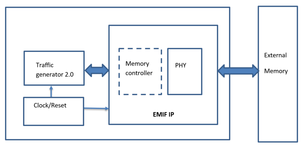
The traffic generator replaces user logic to generate traffic to the external memory. You must incorporate the traffic generator design into the EMIF IP design during IP generation.
When you generate the example design in the parameter editor, the traffic generator module and EMIF IP are generated together. If you have an example design with the Traffic Generator 2.0 enabled, you can configure the traffic pattern using the EMIF Debug Toolkit.
Figure 214. Traffic Generator 2.0 Generated with EMIF IP in Example Design Mode

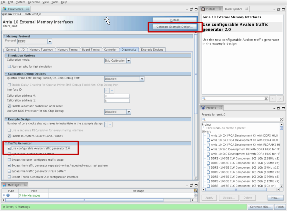
Generating the External Memory Interface
- Select the FPGA and Memory parameters.
- On the Diagnostics tab, configure the following parameters:
- Select Use Configurable Avalon Traffic Generator 2.0.
- Configure the desired traffic pattern, by specifying traffic patterns to be bypassed. The traffic pattern not bypassed is issued to the memory immediately after completion of calibration. You can choose to bypass any of the following traffic patterns:
- Bypass the default traffic pattern Specifies not to use the default traffic patterns from the traffic generator. The default patterns include single read/write, byte-enabled read/write, and block read/write.
- Bypass the user-configured traffic stage. Specifies to skip the stage that uses the user-defined test bench file to configure the traffic generator in simulation.
- Bypass the traffic generator repeated-writes/repeated-reads test pattern. Bypasses the traffic generator's repeat test stage, which causes every write and read to be repeated several times.
- Bypass the traffic generator stress pattern. Bypasses a test stage intended to stress-test signal integrity and memory interface calibration.
- Export Traffic Generator 2.0 configuration interface. Instantiates a port for traffic generator configuration. Use this port if the traffic generator is to be configured by user logic.
- Click Generate Example Design to generate the EMIF IP, including the Traffic Generator 2.0 design, with the traffic pattern that you have configured.
Note: If you click the Generate HDL option instead, the Traffic Generator 2.0 design is not included in the generated IP.
Figure 215. Enabling the Traffic Generator 2.0 in the Parameter Editor

Did you find the information on this page useful?
Feedback Message
Characters remaining: