Quartus® Prime Standard Edition User Guide: Design Compilation
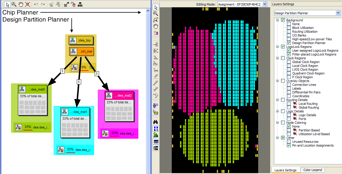
2.6.3. Viewing Design Partition Planner and Floorplan Side-by-Side
To view the Design Partition Planner and Chip Planner side-by-side, open the Design Partition Planner, and then open the Chip Planner and select the Design Partition Planner task. The Design Partition Planner task displays the physical locations of design entities with the same colors as in the Design Partition Planner.
In the Design Partition Planner, you can extract instances of interest from their parents by dragging and dropping, or with the Extract from Parent command. Evaluate the physical locations of instances in the Chip Planner and the connectivity between instances displayed in the Design Partition Planner. An entity is generally not suitable to be set as a separate design partition or constrained in a LogicLock region if the Chip Planner shows it physically dispersed over a noncontiguous area of the device after compilation. Use the Design Partition Planner to analyze the design connections. Child instances that are unsuitable to be set as separate design partitions or placed in LogicLock regions can be returned to their parent by dragging and dropping, or with the Collapse to Parent command.
The figure shows a design displayed in the Design Partition Planner and the Chip Planner with different colors for the top-level design and the three major design instances.