F-tile Architecture and PMA and FEC Direct PHY IP User Guide
A newer version of this document is available. Customers should click here to go to the newest version.
3.3.6. Example Design Generation
The F-Tile PMA/FEC Direct PHY Intel® FPGA IP parameter editor includes the Generate Example Design function to easily create, generate, and simulate the PMA/FEC direct mode example design.
You can select from four Example Design Options for generation, as Figure 66 shows.
The example designs support generation, compilation, and simulation flows for the target device. There is a plan to provide the hardware example design support in an upcoming software release. The following Example Design Options are currently available:
| Example Design Options | Preset Setting Equivalent | Description |
|---|---|---|
| FHT NRZ 25G 1 PMA lane RSFEC 272/258 | FHT_NRZ_25G_1_PMA_Lane_RSFEC_272_258_ED | 1 PMA FHT NRZ lane operating at 25.78125 Gbps with RS-FEC 272/258 mode. |
| FGT NRZ 50G 2 PMA lanes RSFEC 528/514 | FGT_NRZ_50G_2_PMA_Lanes_RSFEC_528_514_ED | 2 PMA FGT NRZ lanes operating at 25.78125 Gbps (each lane) with RS-FEC 528/512 mode. |
| FHT PAM4 4 400G 4 PMA lanes RSFEC 544/514 | FHT_PAM4_400G_4_PMA_lanes_RSFEC_544_514_ED | 4 PMA FHT PAM4 lanes operating at 106.25 Gbps (each lane) with RS-FEC 544/514 mode. |
| FGT NRZ 50G 2 PMA Lanes Custom Cadence | FGT_NRZ_50G_2_PMA_Lanes_Custom_Cadence_ED | 2 PMA FGT NRZ lanes operating at 25.78125 Gbps (each lane) with custom cadence clocking mode. In custom cadence clocking mode, the system PLL clocks the digital data path (that is, the F-tile interface FIFO and core interface FIFO) of the PMA. The PMA block and PMA interface FIFO is clocked by PMA clockout. |
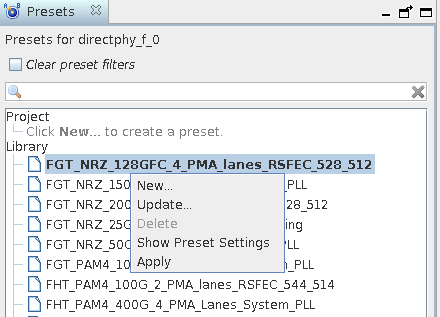
The Example Design Options are equivalent with some of the preset settings, as Table 36 describes. To review the IP parameter settings for each preset, refer to . Alternatively, right-click a preset in the IP parameter editor, and then click Show Preset Settings, or click Apply preset to apply the preset's settings in the parameter editor.
If you select any of the four available Example Design Options, but change the F-Tile PMA/FEC Direct PHY Intel® FPGA IP settings in the GUI thereafter, the example design generated does not follow the changed settings for the F-Tile PMA/FEC Direct PHY Intel® FPGA IP. The example design generation only takes the Example Design Options listed in Table 36. Any other changes that you make to the F-Tile PMA/FEC Direct PHY Intel® FPGA IP settings are not applied during example design generation.
The Example Design tab of the F-Tile PMA/FEC Direct PHY Intel® FPGA IP allows you to select pre-defined RS-FEC options to configure an example design as shown in the following figure.
- FHT NRZ 25G 1 PMA Lane RSFEC 272/25
- FGT NRZ 50G 2 PMA Lanes RSFEC 528/514
- FHT PAM4 4 400G 4 PMA Lanes RSFEC 544/514
- Go to the Example Design tab in the F-Tile PMA/FEC Direct PHY Intel® FPGA IP.
- Select one of the example designs from the drop-down menu. If you select None, you cannot generate the example design.
- Click the Acknowledgment: option box. This options is to remind you that only the example design you specify in the drop-down menu is generated. No other IP parameters setting that you specify take effect in the example design generation. If you do not check the acknowledgment box, you cannot generate the example design.
- Ensure steps 2. and step 3. are done, then click Generate Example Design.
Clicking Generate Example Design completes the IP Generation and Support-logic Generation stages of the Compiler. An example design folder also generates containing the Intel® Quartus® Prime project (.qpf), settings (.qsf), and IP files, simulation, and testbench files for the example design in the following location:
<Project Folder>/<directphy_f_0_example_design/example_design>The Compiler reads the example design .qsf file that contains the PMA reference clock, and the TX and RX high speed serial pin location assignments.
In order to provide a reduction in real-time simulation duration, the example design testbench uses a Fast Sim model. This model is enabled via a macro in the simulation run scripts. The syntax to enable the Fast Sim model is as follows:
+define+IP7581SERDES_UX_SIMSPEEDThis macro is enabled by default in the example design simulation scripts after you click Generate Example Design button.
Example Design Simulation
- To simulate with VCS* , go to the example_design/testbench directory and the launch the simulation using the shell script:
sh run_vcs.sh - To simulate with ModelSim* , go to the example_design/testbench directory and the launch the simulation using the command:
vsim -c -do run_vsim.tcl - Launch waveform viewer to see the simulation results.