External Memory Interfaces Intel® Agilex™ FPGA IP User Guide
A newer version of this document is available. Customers should click here to go to the newest version.
11.10.2. I/O SSM calbus Bridge Data Structures and Usage
At the base of the calbus bridge address range is an array of sub-bank structures, which mimic the physical sub-bank structure (described in the I/O Bank topic in the Architecture chapter of this user guide). The size of the sub-bank structure is 0x0001_0000 bytes, such that sub-bank 0 appears at the base of the calbus bridge, sub-bank 1 is at 0x0301_0000, sub-bank 2 is at 0x0302_0000, and so on.
Each sub-bank structure instantiates four lane structures, a tile center structure, and an hmc structure.
| Address | Structure Type | Structure Instance Name | Description |
|---|---|---|---|
| tile_addr_base_address = 0x0300_0000 + 0x0001_0000*tile_id | lane_struct | lane_0 | Lane data structure, which mimics the physical structure of the lanes within a sub-bank. |
| tile_addr_base_address + 0x2000 | lane_struct | lane_1 | Lane data structure, which mimics the physical structure of the lanes within a sub-bank. |
| tile_addr_base_address + 0x4000 | lane_struct | lane_2 | Lane data structure, which mimics the physical structure of the lanes within a sub-bank. |
| tile_addr_base_address + 0x6000 | lane_struct | lane_3 | Lane data structure, which mimics the physical structure of the lanes within a sub-bank. |
| tile_addr_base_address + 0x8000 | sub_bank_centre_struct | center | Data structure which mimics the physical structure of a tile-center (described in the I/O Bank topic in the Architecture chapter) |
| tile_addr_base_address + 0xA000 | hmc_struct | hmc | Data structure which mimics the physical structure of the MMR space (described in the MMR Tables topic in the End-User Signals chapter. |
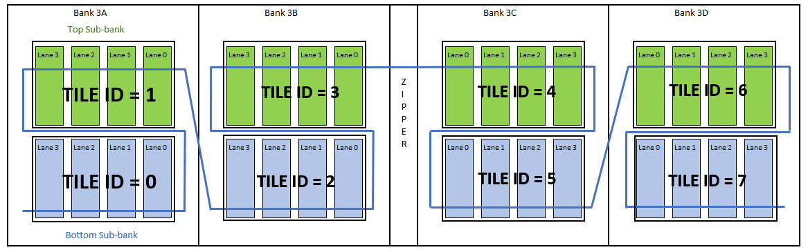
tile_id is the numerical position of a sub-bank when the sub-banks are chained in an I/O row. A tile id value of 0 denotes the bottom sub-bank within the left-most I/O bank.
The following figure depicts the tile IDs for the top I/O row in Intel® Agilex™ AGF012 and AGF014 devices, package R24A.
The lane structure consists of settings for the pins within the lane, as well as settings for the overall lane (such as DQS tree settings).
| Address | Structure Type | Structure Instance Name |
|---|---|---|
| io_lane_addr (base address of lane_0, lane_1, lane_2, or lane_3) | pin_configuration_struct | pin_0 |
| io_lane_addr + 0x0100 | pin_configuration_struct | pin_1 |
| io_lane_addr + 0x0200 | pin_configuration_struct | pin_2 |
| io_lane_addr + 0x0300 | pin_configuration_struct | pin_3 |
| io_lane_addr + 0x0400 | pin_configuration_struct | pin_4 |
| io_lane_addr + 0x0500 | pin_configuration_struct | pin_5 |
| io_lane_addr + 0x0600 | pin_configuration_struct | pin_6 |
| io_lane_addr + 0x0700 | pin_configuration_struct | pin_7 |
| io_lane_addr + 0x0800 | pin_configuration_struct | pin_8 |
| io_lane_addr + 0x0900 | pin_configuration_struct | pin_9 |
| io_lane_addr + 0x0a00 | pin_configuration_struct | pin_10 |
| io_lane_addr + 0x0b00 | pin_configuration_struct | pin_11 |
| io_lane_addr + 0x1800 | dqs_tree_struct | dqs |
| Size (bytes) | Register Name | Description | Offset from Structure Base Address |
|---|---|---|---|
| 4 | reg_counter_b_out | Data Output Delay. | 0xC0 |
| 4 | reg_dqs_toggle_count_clr | DQS Toggle Counter Clear. | 0xCC |
| 4 | reg_out_phase_rank[4] | Data Output Delay Per Rank; each array element corresponds to a memory rank (if applicable). | 0xD0 |
| 4 | reg_io_pin_value | Direct read of pin value. | 0xE4 |
| Size (bytes) | Register Name | Description | Offset from Structure Base Address |
|---|---|---|---|
| 4 | reg_sel_vref | Internal VREF Control (Vref-in). | 0x14 |
| 4 | reg_dq_in_delay_pin0[4] | DQ Input delay of Pin 0; each array element corresponds to a memory rank (if applicable). Bit[12] is the enable bit (enable=1, disable=0). Bit[11:0] is the delay tap. | 0x80 |
| 4 | reg_dq_in_delay_pin1[4] | DQ Input delay of Pin 1; each array element corresponds to a memory rank (if applicable). Bit[12] is the enable bit (enable=1, disable=0). Bit[11:0] is the delay tap. | 0x90 |
| 4 | reg_dq_in_delay_pin2[4] | DQ Input delay of Pin 2; each array element corresponds to a memory rank (if applicable). Bit[12] is the enable bit (enable=1, disable=0). Bit[11:0] is the delay tap. | 0xA0 |
| 4 | reg_dq_in_delay_pin3[4] | DQ Input delay of Pin 3; each array element corresponds to a memory rank (if applicable). Bit[12] is the enable bit (enable=1, disable=0). Bit[11:0] is the delay tap. | 0xB0 |
| 4 | reg_dq_in_delay_pin4[4] | DQ Input delay of Pin 4; each array element corresponds to a memory rank (if applicable). Bit[12] is the enable bit (enable=1, disable=0). Bit[11:0] is the delay tap. | 0xC0 |
| 4 | reg_dq_in_delay_pin5[4] | DQ Input delay of Pin 5; each array element corresponds to a memory rank (if applicable). Bit[12] is the enable bit (enable=1, disable=0). Bit[11:0] is the delay tap. | 0xD0 |
| 4 | reg_dqs_in_delay_a[4] | DQS input delay A; each array element corresponds to a memory rank (if applicable). Bit[12] is the enable bit (enable=1, disable=0). Bit[11:0] is the delay tap. | 0xE0 |
| 4 | reg_dqs_preamble_delay_a[4] | DQS preamble input delay A; each array element corresponds to a memory rank (if applicable). Bit[15] is the enable bit (enable=1, disable=0). Bit[11:0] is the delay tap. | 0xF0 |
| 4 | reg_dq_in_delay_pin6[4] | DQ Input delay of Pin 6; each array element corresponds to a memory rank (if applicable). Bit[12] is the enable bit (enable=1, disable=0). Bit[11:0] is the delay tap. | 0x100 |
| 4 | reg_dq_in_delay_pin7[4] | DQ Input delay of Pin 7; each array element corresponds to a memory rank (if applicable). Bit[12] is the enable bit (enable=1, disable=0). Bit[11:0] is the delay tap. | 0x110 |
| 4 | reg_dq_in_delay_pin8[4] | DQ Input delay of Pin 8; each array element corresponds to a memory rank (if applicable). Bit[12] is the enable bit (enable=1, disable=0). Bit[11:0] is the delay tap. | 0x120 |
| 4 | reg_dq_in_delay_pin9[4] | DQ Input delay of Pin 9; each array element corresponds to a memory rank (if applicable). Bit[12] is the enable bit (enable=1, disable=0). Bit[11:0] is the delay tap. | 0x130 |
| 4 | reg_dq_in_delay_pin10[4] | DQ Input delay of Pin 10; each array element corresponds to a memory rank (if applicable). Bit[12] is the enable bit (enable=1, disable=0). Bit[11:0] is the delay tap. | 0x140 |
| 4 | reg_dq_in_delay_pin11[4] | DQ Input delay of Pin 11; each array element corresponds to a memory rank (if applicable). Bit[12] is the enable bit (enable=1, disable=0). Bit[11:0] is the delay tap. | 0x150 |
| 4 | reg_dqs_in_delay_b[4] | DQS input delay B; each array element corresponds to a memory rank (if applicable). Bit[12] is the enable bit (enable=1, disable=0). Bit[11:0] is the delay tap. | 0x160 |
| 4 | reg_dqs_preamble_delay_b[4] | DQS preamble input delay B; each array element corresponds to a memory rank (if applicable). Bit[15] is the enable bit (enable=1, disable=0). Bit[11:0] is the delay tap. | 0x170 |