PHY Lite for Parallel Interfaces Intel® FPGA IP User Guide
A newer version of this document is available. Customers should click here to go to the newest version.
3.6.1.2.1. Dynamic Reconfiguration Using Finite State Machine
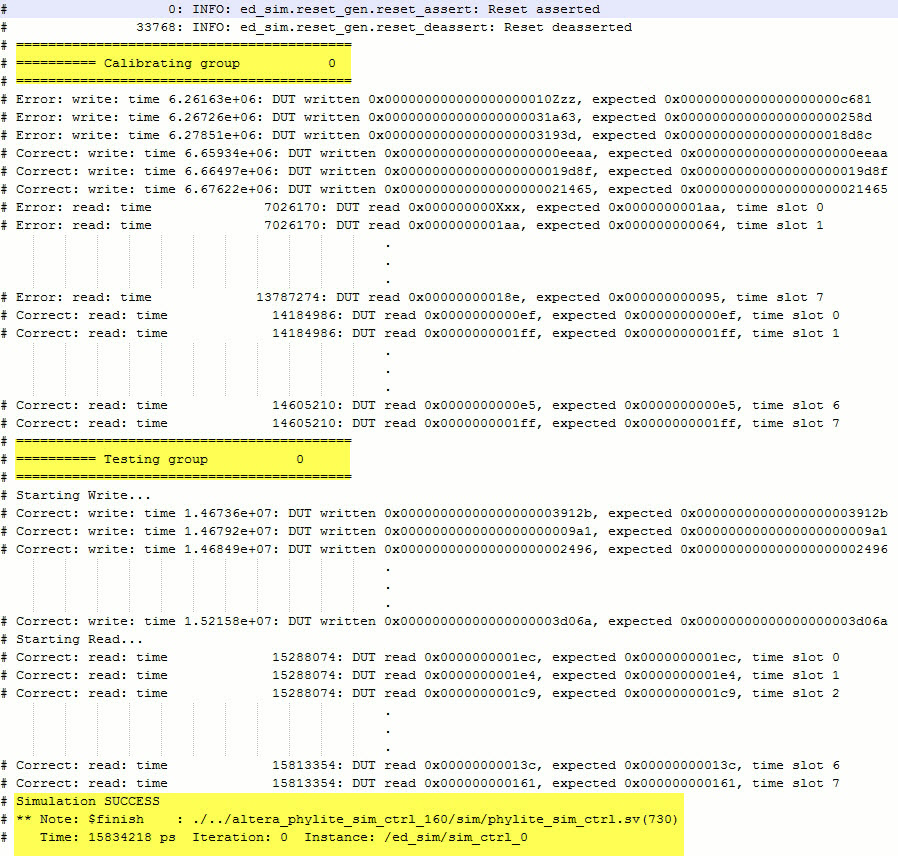
This design example is a simulation design example that is capable to perform dynamic calibration for PHY Lite for Parallel Interfaces Intel® Stratix® 10 FPGA IP.
Features
- Perform dynamic reconfiguration using Avalon controller
- Read and write transactions monitoring
- Delay values monitoring
Software Requirements
- Intel® Quartus® Prime software
- Active-HDL, ModelSim* - Intel® FPGA Edition, or VCS Simulator
Functional Description
This design example introduces the cfg_ctrl and avl_ctrl blocks, which work with the sim_ctrl module to demonstrate the basic functionality of the PHY Lite for Parallel Interfaces Intel® Stratix® 10 FPGA IP Avalon memory-mapped based reconfiguration. The agent is also modified to insert delays on the data and clocks, which the new modules will compensate for.
NOTE: The cfg_ctrl module performs a simplistic reconfiguration of the interface that stops at the first working delay values. The design example only support simulation. A robust calibration algorithm should sweep over the entire valid range of delays to choose the correct value for the application.
| Component | Description |
|---|---|
| ref_clk_gen | Generates clock to reset_gen, PHY Lite for Parallel Interfaces Intel® Stratix® 10 FPGA IP ADDR/CMD (ref_clk), and PHY Lite for Parallel Interfaces Intel® Stratix® 10 FPGA IP (ref_clk) blocks. |
| reset_gen | Generates reset to PHY Lite for Parallel Interfaces ADDR/CMD and PHY Lite for Parallel Interfaces Intel® Stratix® 10 FPGA IP blocks. |
| sim_ctrl |
|
| Driver | Generates strobe and data for each group and to PHY Lite for Parallel Interfaces_ Intel® Stratix® 10 FPGA IP block. |
| PHY Lite for Parallel Interfaces ADDR/CMD | Passing read/write commands and command clock from sim_ctrl to Agent. |
| Agent | FIFO to store data from PHY Lite for Parallel Interfaces DUT and side read/write data from sim_ctrl block. |
| cfg_ctrl | This is configuration control block which performs read and write delay calibration before test begin. The calibration results is passed to the PHY Lite for Parallel Interfaces Intel® Stratix® 10 FPGA IP through Avalon Controller. Contains 4 FSMs:
|
| avl_ctrl | The Avalon controller is used to perform address translation to store delay settings from the calibration done by cfg_ctrl block. |
Generate the Dynamic Reconfiguration with Configuration Control Module Design Example
- In Intel® Quartus® Prime software, instantiate PHY Lite for Parallel Interfaces IP core.
- Customize parameter settings per your requirement and turn on the Use dynamic reconfiguration option.
- Click Generate Example Design. Specify a directory name to generate the design example.
- To generate Verilog or mixed-language simulation files, go to the design example directory and run the following script in Nios II Command Shell.
quartus_sh -t make_sim_design.tcl VERILOG - To generate VHDL simulation files, go to the design example directory and run the following script in Nios II Command Shell.
quartus_sh -t make_sim_design.tcl VHDL
Run the Dynamic Reconfiguration with Configuration Control Design Example
Follow these steps to compile and simulate the design:
- Change the working directory to <Example Design>\sim\ed_sim\sim\<Simulator> .
- Run the simulation script for the simulator of your choice. Refer to the table below.
Simulator Working Directory Steps Modelsim <Example Design>\sim\ed_sim\sim\mentor - do msim_setup.tcl
- ld_debug
- Add desired signals into the waveform window.
- run -all
VCS <Example Design>\sim\ed_sim\sim\synopsys\vcs - sh vcs_setup.sh
VCSMX <Example Design>\sim\ed_sim\sim\synopsys\vcsmx - sh vcsmx_setup.sh
Aldec Example Design\sim\ed_sim\sim\aldec - do rivierapro_setup.tcl
- ld_debug
- Add desired signals into the waveform window.
- run -all