External Memory Interfaces Intel® Stratix® 10 FPGA IP User Guide
ID
683741
Date
9/26/2022
Public
A newer version of this document is available. Customers should click here to go to the newest version.
1. Release Information
2. External Memory Interfaces Intel® Stratix® 10 FPGA IP Introduction
3. Intel® Stratix® 10 EMIF IP Product Architecture
4. Intel® Stratix® 10 EMIF IP End-User Signals
5. Intel® Stratix® 10 EMIF – Simulating Memory IP
6. Intel® Stratix® 10 EMIF IP for DDR3
7. Intel® Stratix® 10 EMIF IP for DDR4
8. Intel® Stratix® 10 EMIF IP for QDR II/II+/II+ Xtreme
9. Intel® Stratix® 10 EMIF IP for QDR-IV
10. Intel® Stratix® 10 EMIF IP for RLDRAM 3
11. Intel® Stratix® 10 EMIF IP Timing Closure
12. Optimizing Controller Performance
13. Intel® Stratix® 10 EMIF IP Debugging
14. External Memory Interfaces Intel® Stratix® 10 FPGA IP User Guide Archives
15. Document Revision History for External Memory Interfaces Intel® Stratix® 10 FPGA IP User Guide
3.1. Intel® Stratix® 10 EMIF Architecture: Introduction
3.2. Intel® Stratix® 10 EMIF Sequencer
3.3. Intel® Stratix® 10 EMIF Calibration
3.4. Intel Stratix 10 EMIF IP Controller
3.5. Hardware Resource Sharing Among Multiple Intel® Stratix® 10 EMIFs
3.6. User-requested Reset in Intel® Stratix® 10 EMIF IP
3.7. Intel® Stratix® 10 EMIF for Hard Processor Subsystem
3.8. Intel® Stratix® 10 EMIF Ping Pong PHY
3.1.1. Intel® Stratix® 10 EMIF Architecture: I/O Subsystem
3.1.2. Intel® Stratix® 10 EMIF Architecture: I/O Column
3.1.3. Intel® Stratix® 10 EMIF Architecture: I/O SSM
3.1.4. Intel® Stratix® 10 EMIF Architecture: I/O Bank
3.1.5. Intel® Stratix® 10 EMIF Architecture: I/O Lane
3.1.6. Intel® Stratix® 10 EMIF Architecture: Input DQS Clock Tree
3.1.7. Intel® Stratix® 10 EMIF Architecture: PHY Clock Tree
3.1.8. Intel® Stratix® 10 EMIF Architecture: PLL Reference Clock Networks
3.1.9. Intel® Stratix® 10 EMIF Architecture: Clock Phase Alignment
4.1.1.1. local_reset_req for DDR3
4.1.1.2. local_reset_status for DDR3
4.1.1.3. pll_ref_clk for DDR3
4.1.1.4. pll_locked for DDR3
4.1.1.5. pll_extra_clk_0 for DDR3
4.1.1.6. pll_extra_clk_1 for DDR3
4.1.1.7. pll_extra_clk_2 for DDR3
4.1.1.8. pll_extra_clk_3 for DDR3
4.1.1.9. oct for DDR3
4.1.1.10. mem for DDR3
4.1.1.11. status for DDR3
4.1.1.12. afi_reset_n for DDR3
4.1.1.13. afi_clk for DDR3
4.1.1.14. afi_half_clk for DDR3
4.1.1.15. afi for DDR3
4.1.1.16. emif_usr_reset_n for DDR3
4.1.1.17. emif_usr_clk for DDR3
4.1.1.18. emif_usr_reset_n_sec for DDR3
4.1.1.19. emif_usr_clk_sec for DDR3
4.1.1.20. cal_debug_reset_n for DDR3
4.1.1.21. cal_debug_clk for DDR3
4.1.1.22. cal_debug_out_reset_n for DDR3
4.1.1.23. cal_debug_out_clk for DDR3
4.1.1.24. clks_sharing_master_out for DDR3
4.1.1.25. clks_sharing_slave_in for DDR3
4.1.1.26. clks_sharing_slave_out for DDR3
4.1.1.27. ctrl_amm for DDR3
4.1.1.28. ctrl_auto_precharge for DDR3
4.1.1.29. ctrl_user_priority for DDR3
4.1.1.30. ctrl_ecc_user_interrupt for DDR3
4.1.1.31. ctrl_ecc_readdataerror for DDR3
4.1.1.32. ctrl_ecc_status for DDR3
4.1.1.33. ctrl_mmr_slave for DDR3
4.1.1.34. hps_emif for DDR3
4.1.1.35. cal_debug for DDR3
4.1.1.36. cal_debug_out for DDR3
4.1.2.1. local_reset_req for DDR4
4.1.2.2. local_reset_status for DDR4
4.1.2.3. pll_ref_clk for DDR4
4.1.2.4. pll_locked for DDR4
4.1.2.5. pll_extra_clk_0 for DDR4
4.1.2.6. pll_extra_clk_1 for DDR4
4.1.2.7. pll_extra_clk_2 for DDR4
4.1.2.8. pll_extra_clk_3 for DDR4
4.1.2.9. ac_parity_err for DDR4
4.1.2.10. oct for DDR4
4.1.2.11. mem for DDR4
4.1.2.12. status for DDR4
4.1.2.13. afi_reset_n for DDR4
4.1.2.14. afi_clk for DDR4
4.1.2.15. afi_half_clk for DDR4
4.1.2.16. afi for DDR4
4.1.2.17. emif_usr_reset_n for DDR4
4.1.2.18. emif_usr_clk for DDR4
4.1.2.19. emif_usr_reset_n_sec for DDR4
4.1.2.20. emif_usr_clk_sec for DDR4
4.1.2.21. cal_debug_reset_n for DDR4
4.1.2.22. cal_debug_clk for DDR4
4.1.2.23. cal_debug_out_reset_n for DDR4
4.1.2.24. cal_debug_out_clk for DDR4
4.1.2.25. clks_sharing_master_out for DDR4
4.1.2.26. clks_sharing_slave_in for DDR4
4.1.2.27. clks_sharing_slave_out for DDR4
4.1.2.28. ctrl_amm for DDR4
4.1.2.29. ctrl_auto_precharge for DDR4
4.1.2.30. ctrl_user_priority for DDR4
4.1.2.31. ctrl_ecc_user_interrupt for DDR4
4.1.2.32. ctrl_ecc_readdataerror for DDR4
4.1.2.33. ctrl_ecc_status for DDR4
4.1.2.34. ctrl_mmr_slave for DDR4
4.1.2.35. hps_emif for DDR4
4.1.2.36. cal_debug for DDR4
4.1.2.37. cal_debug_out for DDR4
4.1.3.1. local_reset_req for QDR II/II+/II+ Xtreme
4.1.3.2. local_reset_status for QDR II/II+/II+ Xtreme
4.1.3.3. pll_ref_clk for QDR II/II+/II+ Xtreme
4.1.3.4. pll_locked for QDR II/II+/II+ Xtreme
4.1.3.5. pll_extra_clk_0 for QDR II/II+/II+ Xtreme
4.1.3.6. pll_extra_clk_1 for QDR II/II+/II+ Xtreme
4.1.3.7. pll_extra_clk_2 for QDR II/II+/II+ Xtreme
4.1.3.8. pll_extra_clk_3 for QDR II/II+/II+ Xtreme
4.1.3.9. oct for QDR II/II+/II+ Xtreme
4.1.3.10. mem for QDR II/II+/II+ Xtreme
4.1.3.11. status for QDR II/II+/II+ Xtreme
4.1.3.12. emif_usr_reset_n for QDR II/II+/II+ Xtreme
4.1.3.13. emif_usr_clk for QDR II/II+/II+ Xtreme
4.1.3.14. cal_debug_reset_n for QDR II/II+/II+ Xtreme
4.1.3.15. cal_debug_clk for QDR II/II+/II+ Xtreme
4.1.3.16. cal_debug_out_reset_n for QDR II/II+/II+ Xtreme
4.1.3.17. cal_debug_out_clk for QDR II/II+/II+ Xtreme
4.1.3.18. clks_sharing_master_out for QDR II/II+/II+ Xtreme
4.1.3.19. clks_sharing_slave_in for QDR II/II+/II+ Xtreme
4.1.3.20. clks_sharing_slave_out for QDR II/II+/II+ Xtreme
4.1.3.21. ctrl_amm for QDR II/II+/II+ Xtreme
4.1.3.22. cal_debug for QDR II/II+/II+ Xtreme
4.1.3.23. cal_debug_out for QDR II/II+/II+ Xtreme
4.1.4.1. local_reset_req for QDR-IV
4.1.4.2. local_reset_status for QDR-IV
4.1.4.3. pll_ref_clk for QDR-IV
4.1.4.4. pll_locked for QDR-IV
4.1.4.5. pll_extra_clk_0 for QDR-IV
4.1.4.6. pll_extra_clk_1 for QDR-IV
4.1.4.7. pll_extra_clk_2 for QDR-IV
4.1.4.8. pll_extra_clk_3 for QDR-IV
4.1.4.9. oct for QDR-IV
4.1.4.10. mem for QDR-IV
4.1.4.11. status for QDR-IV
4.1.4.12. afi_reset_n for QDR-IV
4.1.4.13. afi_clk for QDR-IV
4.1.4.14. afi_half_clk for QDR-IV
4.1.4.15. afi for QDR-IV
4.1.4.16. emif_usr_reset_n for QDR-IV
4.1.4.17. emif_usr_clk for QDR-IV
4.1.4.18. cal_debug_reset_n for QDR-IV
4.1.4.19. cal_debug_clk for QDR-IV
4.1.4.20. cal_debug_out_reset_n for QDR-IV
4.1.4.21. cal_debug_out_clk for QDR-IV
4.1.4.22. clks_sharing_master_out for QDR-IV
4.1.4.23. clks_sharing_slave_in for QDR-IV
4.1.4.24. clks_sharing_slave_out for QDR-IV
4.1.4.25. ctrl_amm for QDR-IV
4.1.4.26. cal_debug for QDR-IV
4.1.4.27. cal_debug_out for QDR-IV
4.1.5.1. local_reset_req for RLDRAM 3
4.1.5.2. local_reset_status for RLDRAM 3
4.1.5.3. pll_ref_clk for RLDRAM 3
4.1.5.4. pll_locked for RLDRAM 3
4.1.5.5. pll_extra_clk_0 for RLDRAM 3
4.1.5.6. pll_extra_clk_1 for RLDRAM 3
4.1.5.7. pll_extra_clk_2 for RLDRAM 3
4.1.5.8. pll_extra_clk_3 for RLDRAM 3
4.1.5.9. oct for RLDRAM 3
4.1.5.10. mem for RLDRAM 3
4.1.5.11. status for RLDRAM 3
4.1.5.12. afi_reset_n for RLDRAM 3
4.1.5.13. afi_clk for RLDRAM 3
4.1.5.14. afi_half_clk for RLDRAM 3
4.1.5.15. afi for RLDRAM 3
4.1.5.16. cal_debug_reset_n for RLDRAM 3
4.1.5.17. cal_debug_clk for RLDRAM 3
4.1.5.18. cal_debug_out_reset_n for RLDRAM 3
4.1.5.19. cal_debug_out_clk for RLDRAM 3
4.1.5.20. clks_sharing_master_out for RLDRAM 3
4.1.5.21. clks_sharing_slave_in for RLDRAM 3
4.1.5.22. clks_sharing_slave_out for RLDRAM 3
4.1.5.23. cal_debug for RLDRAM 3
4.1.5.24. cal_debug_out for RLDRAM 3
4.4.1. ctrlcfg0
4.4.2. ctrlcfg1
4.4.3. dramtiming0
4.4.4. caltiming0
4.4.5. caltiming1
4.4.6. caltiming2
4.4.7. caltiming3
4.4.8. caltiming4
4.4.9. caltiming9
4.4.10. dramaddrw
4.4.11. sideband0
4.4.12. sideband1
4.4.13. sideband4
4.4.14. sideband6
4.4.15. sideband7
4.4.16. sideband9
4.4.17. sideband11
4.4.18. sideband12
4.4.19. sideband13
4.4.20. sideband14
4.4.21. dramsts
4.4.22. niosreserve0
4.4.23. niosreserve1
4.4.24. sideband16
4.4.25. ecc3: ECC Error and Interrupt Configuration
4.4.26. ecc4: Status and Error Information
4.4.27. ecc5: Address of Most Recent SBE/DBE
4.4.28. ecc6: Address of Most Recent Correction Command Dropped
4.4.29. ecc7: Extension for Address of Most Recent SBE/DBE
4.4.30. ecc8: Extension for Address of Most Recent Correction Command Dropped
6.1.1. Intel Stratix 10 EMIF IP DDR3 Parameters: General
6.1.2. Intel Stratix 10 EMIF IP DDR3 Parameters: FPGA I/O
6.1.3. Intel Stratix 10 EMIF IP DDR3 Parameters: Memory
6.1.4. Intel Stratix 10 EMIF IP DDR3 Parameters: Mem I/O
6.1.5. Intel Stratix 10 EMIF IP DDR3 Parameters: Mem Timing
6.1.6. Intel Stratix 10 EMIF IP DDR3 Parameters: Board
6.1.7. Intel Stratix 10 EMIF IP DDR3 Parameters: Controller
6.1.8. Intel Stratix 10 EMIF IP DDR3 Parameters: Diagnostics
6.1.9. Intel Stratix 10 EMIF IP DDR3 Parameters: Example Designs
7.1.1. Intel Stratix 10 EMIF IP DDR4 Parameters: General
7.1.2. Intel Stratix 10 EMIF IP DDR4 Parameters: FPGA I/O
7.1.3. Intel Stratix 10 EMIF IP DDR4 Parameters: Memory
7.1.4. Intel Stratix 10 EMIF IP DDR4 Parameters: Mem I/O
7.1.5. Intel Stratix 10 EMIF IP DDR4 Parameters: Mem Timing
7.1.6. Intel Stratix 10 EMIF IP DDR4 Parameters: Board
7.1.7. Intel Stratix 10 EMIF IP DDR4 Parameters: Controller
7.1.8. Intel Stratix 10 EMIF IP DDR4 Parameters: Diagnostics
7.1.9. Intel Stratix 10 EMIF IP DDR4 Parameters: Example Designs
7.5.4.1. General Layout Guidelines
7.5.4.2. Layout Guidelines
7.5.4.3. Length Matching Rules
7.5.4.4. Spacing Guidelines
7.5.4.5. Layout Guidelines for DDR3 and DDR4 SDRAM Wide Interface (>72 bits)
7.5.4.6. Fly-By Network Design for Clock, Command, and Address Signals
7.5.4.7. Clamshell Topology
7.5.4.8. Additional Layout Guidelines for DDR4 Twin-die Devices
8.1.1. Intel Stratix 10 EMIF IP QDR II/II+/II+ Xtreme Parameters: General
8.1.2. Intel Stratix 10 EMIF IP QDR II/II+/II+ Xtreme Parameters: FPGA I/O
8.1.3. Intel Stratix 10 EMIF IP QDR II/II+/II+ Xtreme Parameters: Memory
8.1.4. Intel Stratix 10 EMIF IP QDR II/II+/II+ Xtreme Parameters: Mem Timing
8.1.5. Intel Stratix 10 EMIF IP QDR II/II+/II+ Xtreme Parameters: Board
8.1.6. Intel Stratix 10 EMIF IP QDR II/II+/II+ Xtreme Parameters: Controller
8.1.7. Intel Stratix 10 EMIF IP QDR II/II+/II+ Xtreme Parameters: Diagnostics
8.1.8. Intel Stratix 10 EMIF IP QDR II/II+/II+ Xtreme Parameters: Example Designs
8.3.1.6.1. General Guidelines
8.3.1.6.2. QDR II, QDR II+ and QDR II+ Xtreme SRAM Command Signals
8.3.1.6.3. QDR II, QDR II+ and QDR II+ Xtreme SRAM Address Signals
8.3.1.6.4. QDR II, QDR II+, and QDR II+ Xtreme SRAM Clock Signals
8.3.1.6.5. QDR II, QDR II+ and QDR II+ Xtreme SRAM Data, BWS, and QVLD Signals
8.3.1.6.6. Resource Sharing Guidelines (Multiple Interfaces)
9.1.1. Intel Stratix 10 EMIF IP QDR-IV Parameters: General
9.1.2. Intel Stratix 10 EMIF IP QDR-IV Parameters: FPGA I/O
9.1.3. Intel Stratix 10 EMIF IP QDR-IV Parameters: Memory
9.1.4. Intel Stratix 10 EMIF IP QDR-IV Parameters: Mem Timing
9.1.5. Intel Stratix 10 EMIF IP QDR-IV Parameters: Board
9.1.6. Intel Stratix 10 EMIF IP QDR-IV Parameters: Controller
9.1.7. Intel Stratix 10 EMIF IP QDR-IV Parameters: Diagnostics
9.1.8. Intel Stratix 10 EMIF IP QDR-IV Parameters: Example Designs
10.1.1. Intel Stratix 10 EMIF IP RLDRAM 3 Parameters: General
10.1.2. Intel Stratix 10 EMIF IP RLDRAM 3 Parameters: FPGA I/O
10.1.3. Intel Stratix 10 EMIF IP RLDRAM 3 Parameters: Memory
10.1.4. Intel Stratix 10 EMIF IP RLDRAM 3 Parameters: Mem Timing
10.1.5. Intel Stratix 10 EMIF IP RLDRAM 3 Parameters: Board
10.1.6. Intel Stratix 10 EMIF IP RLDRAM 3 Parameters: Diagnostics
10.1.7. Intel Stratix 10 EMIF IP RLDRAM 3 Parameters: Example Designs
12.4.1. Auto-Precharge Commands
12.4.2. Latency
12.4.3. Calibration
12.4.4. Bank Interleaving
12.4.5. Additive Latency and Bank Interleaving
12.4.6. User-Controlled Refresh
12.4.7. Frequency of Operation
12.4.8. Series of Reads or Writes
12.4.9. Data Reordering
12.4.10. Starvation Control
12.4.11. Command Reordering
12.4.12. Bandwidth
12.4.13. Enable Command Priority Control
13.1. Interface Configuration Performance Issues
13.2. Functional Issue Evaluation
13.3. Timing Issue Characteristics
13.4. Verifying Memory IP Using the Signal Tap II Logic Analyzer
13.5. Hardware Debugging Guidelines
13.6. Categorizing Hardware Issues
13.7. Debugging Intel® Stratix® 10 EMIF IP
13.8. Using the Default Traffic Generator
13.9. Using the Configurable Traffic Generator (TG2)
13.5.1. Create a Simplified Design that Demonstrates the Same Issue
13.5.2. Measure Power Distribution Network
13.5.3. Measure Signal Integrity and Setup and Hold Margin
13.5.4. Vary Voltage
13.5.5. Operate at a Lower Speed
13.5.6. Determine Whether the Issue Exists in Previous Versions of Software
13.5.7. Determine Whether the Issue Exists in the Current Version of Software
13.5.8. Try A Different PCB
13.5.9. Try Other Configurations
13.5.10. Debugging Checklist
13.7.1. Debugging With the Legacy External Memory Interface Debug Toolkit
13.7.2. Debugging with the External Memory Interface Unified Calibration Debug Toolkit
13.7.3. On-Chip Debug Port for Intel® Stratix® 10 EMIF IP
13.7.4. Legacy Efficiency Monitor and Protocol Checker
13.7.5. New Efficiency Monitor
13.7.1.1. User Interface
13.7.1.2. Communication
13.7.1.3. Setup and Use
13.7.1.4. Configuring Your EMIF IP for Use with the Legacy Debug Toolkit
13.7.1.5. Reports
13.7.1.6. On-Die Termination Calibration
13.7.1.7. Eye Diagram
13.7.1.8. Driver Margining for Intel® Stratix® 10 EMIF IP
13.7.1.9. Example Tcl Script for Running the Legacy EMIF Debug Toolkit
13.7.1.10. Using the Legacy EMIF Debug Toolkit with Intel® Stratix® 10 HPS Interfaces
13.7.2.1. Prerequisites for Using the EMIF Unified Calibration Debug Toolkit
13.7.2.2. Configuring a Design to use the EMIF Unified Calibration Debug Toolkit
13.7.2.3. Launching the EMIF Debug Toolkit
13.7.2.4. Using the EMIF Debug Toolkit
13.7.2.5. Exporting Tables
13.7.2.6. Viewing Diagrams in the Eye Viewer
13.7.2.7. Guidelines for Debugging Calibration Issues
13.7.2.7.1. Debugging Calibration Failure Using Information from the Calibration report
13.7.2.7.2. Debugging Address and Command Leveling Calibration Failure
13.7.2.7.3. Debugging Address and Command Deskew Failure
13.7.2.7.4. Debugging DQS Enable Failure
13.7.2.7.5. Debugging Read Deskew Calibration Failure
13.7.2.7.6. Debugging VREFIN Calibration Failure
13.7.2.7.7. Debugging LFIFO Calibration Failure
13.7.2.7.8. Debugging Write Leveling Failure
13.7.2.7.9. Debugging Write Deskew Calibration Failure
13.7.2.7.10. Debugging VREFOUT Calibration Failure
13.9.1. Enabling the Traffic Generator in a Design Example
13.9.2. Traffic Generator Block Description
13.9.3. Default Traffic Pattern
13.9.4. Configuration and Status Registers
13.9.5. User Pattern
13.9.6. Traffic Generator Status
13.9.7. Starting Traffic with the Traffic Generator
13.9.8. Traffic Generator Configuration User Interface
13.9.9. Examples of Configuring the TG2 Traffic Generator
11.1.1.2.3. Address and Command
Address and command signals are single data rate signals latched by the memory device using the FPGA output clock; some are half-rate data signals, while others, such as the chip select, are full-rate signals.
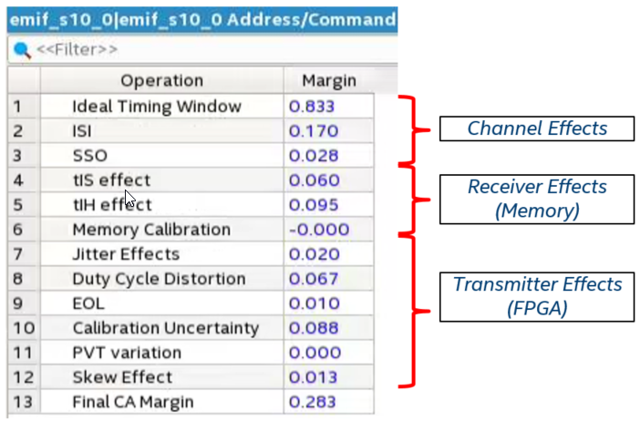
The Timing Analyzer analyzes the address and command timing paths through conventional static timing analysis and further processing steps that account for memory pessimism removal (as shown in the following figure). Depending on the memory protocol in use, if address command calibration is performed, calibration uncertainty is subtracted from the timing window while PVT variation and skew effects are not subtracted, and vice versa.
Figure 90. Address and Command Timing Analysis