1. About the Video and Vision Processing Suite
2. Getting Started with the Video and Vision Processing IPs
3. Video and Vision Processing IPs Functional Description
4. Video and Vision Processing IP Interfaces
5. Video and Vision Processing IP Registers
6. Video and Vision Processing IPs Software Programming Model
7. Protocol Converter IP
8. 1D LUT IP
9. 3D LUT IP
10. Adaptive Noise Reduction IP
11. Advanced Test Pattern Generator IP
12. AXI-Stream Broadcaster IP
13. Bits per Color Sample Adapter IP
14. Black Level Correction IP
15. Black Level Statistics IP
16. Chroma Key IP
17. Chroma Resampler IP
18. Clipper IP
19. Clocked Video Input IP
20. Clocked Video to Full-Raster Converter IP
21. Clocked Video Output IP
22. Color Plane Manager IP
23. Color Space Converter IP
24. Defective Pixel Correction IP
25. Deinterlacer IP
26. Demosaic IP
27. FIR Filter IP
28. Frame Cleaner IP
29. Full-Raster to Clocked Video Converter IP
30. Full-Raster to Streaming Converter IP
31. Genlock Controller IP
32. Generic Crosspoint IP
33. Genlock Signal Router IP
34. Guard Bands IP
35. Histogram Statistics IP
36. Interlacer IP
37. Mixer IP
38. Pixels in Parallel Converter IP
39. Scaler IP
40. Stream Cleaner IP
41. Switch IP
42. Text Box IP
43. Tone Mapping Operator IP
44. Test Pattern Generator IP
45. Unsharp Mask IP
46. Video and Vision Monitor Intel FPGA IP
47. Video Frame Buffer IP
48. Video Frame Reader Intel FPGA IP
49. Video Frame Writer Intel FPGA IP
50. Video Streaming FIFO IP
51. Video Timing Generator IP
52. Vignette Correction IP
53. Warp IP
54. White Balance Correction IP
55. White Balance Statistics IP
56. Design Security
57. Document Revision History for Video and Vision Processing Suite User Guide
31.4.1. Achieving Genlock Controller Free Running (for Initialization or from Lock to Reference Clock N)
31.4.2. Locking to Reference Clock N (from Genlock Controller IP free running)
31.4.3. Setting the VCXO hold over
31.4.4. Restarting the Genlock Controller IP
31.4.5. Locking to Reference Clock N New (from Locking to Reference Clock N Old)
31.4.6. Changing to Reference Clock or VCXO Base Frequencies (switch between p50 and p59.94 video formats and vice-versa)
31.4.7. Disturbing a Reference Clock (a cable pull)
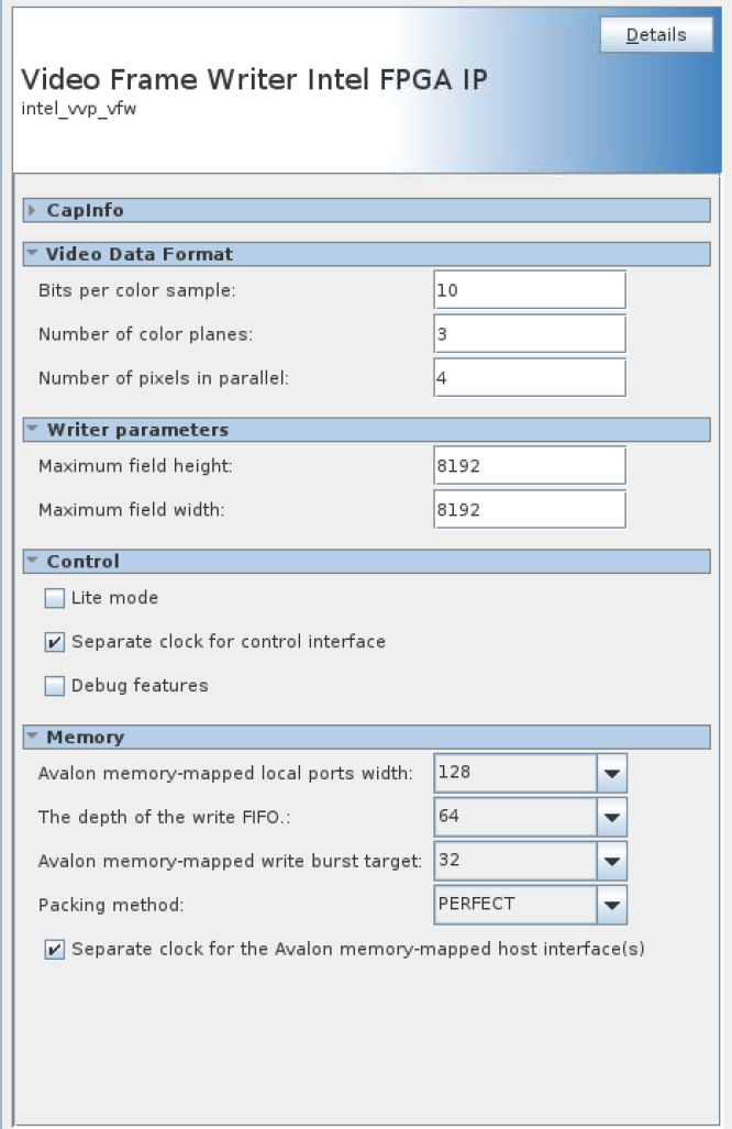
49.2. Video Frame Writer IP Parameters
The IP offers compile-time parameters.
| Parameter | Values | Description | |||
|---|---|---|---|---|---|
| Video Data Format | |||||
| Bits per color sample | 8 to 16 | Select the number of bits per color sample. | |||
| Number of color planes | 1 to 4 | Select the number of color planes per pixel. | |||
| Number of pixels in parallel | 1 to 8 | Select the number of pixels in parallel. | |||
| Maximum Frame Size | |||||
| Maximum frame height | 32 to 16384 | Select the maximum height of frames. If you attempt to write fields or frames taller than this, they are cropped to this height. | |||
| Maximum frame width | 32 to 16384 | Select the maximum width of frames. If you attempt to write fields or frames wider than this, they are cropped to this width. If you use the IP exclusively to write frames with 420 subsampling, optionally, halve the maximum frame width entry in the GUI. Halving the entry optimizes memory footprint because of the more efficient 420 pixel packing. |
|||
| Control | |||||
| Lite mode | On or off | Turn on to operate the frame writer in lite mode. | |||
| Separate clock for control interface | On or off | Turn on for a separate clock for the control interface. | |||
| Debug features | On or off | Turn on for debug features. | |||
| Memory | |||||
| Avalon memory mapped host(s) local ports width | 16, 32, 64, 128, 256, 512, 1024 | Select in bits the width of the Avalon memory-mapped host write port. You must select a width at least as wide as the Intel streaming video input tdata width. | |||
| Avalon memory mapped host(s) local ports address width | 8 to 32 | Select in bits the width of the Avalon memory-mapped host write address port. It must be sufficient to fully address the last buffer. | |||
| The depth of the write FIFO | 32,64,128,256,512,1024,2048 | Specify the depth of the write FIFO buffer. Each FIFO buffer entry holds one word the width of the specified Avalon memory-mapped local port width. You must specify a FIFO depth of at least twice the specified burst target so that the IP can hold at least 2 bursts at any one time. Increase the FIFO depth to improve resilience to latency on the Avalon memory-mapped interface. | |||
| Avalon memory mapped write burst target | 2,4,8,16,32,64 | Select the burst target for writes. Longer bursts provide more efficiency on the bus but require more local storage in the write FIFO buffer. | |||
| Packing method | Perfect, color or pixel | Perfect packing minimizes memory footprint of stored frames but increases complexity and therefore size of the frame writer slightly. Color packing leaves spaces in memory between colors if colors do not pack into memory words exactly. Pixel packing leaves spaces in memory between pixels if pixels do not pack into memory words exactly. | |||
| Separate clock for the Avalon memory-mapped host interface(s) | On or off | - | |||
Figure 131. Frame Writer IP GUI