49.3. Video Frame Writer IP Functional Description
- Configure the IP with the number of buffers that you want to write to with the csr_num_buffers register.
- Program the base address in memory for the first buffer, the offset between buffers and the offset between individual lines within buffers via the csr_buffer_base, csr_inter_buffer_offset and csr_inter_line_offset registers.
- Set the csr_overwrite_broken register if you want broken frames to be overwritten and then csr_run to either free-running mode for continuous operation or single-shot mode.
- Commit these settings with a write to the csr_commit register.
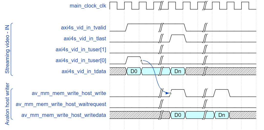
If the IP receives any packets on its Intel FPGA streaming video input before you configure and commit it, the IP consumes the packets. When consuming, the IP raises axi4s_vid_in_tready.
Register Behavior
Bit [0] of the csr_status register goes high when the IP starts writing the first frame. It goes low after the IP finishes writing the last line of the frame. It returns high when the IP starts writing the next frame.
The IP sets the csr_buffer_available register after it writes the first frame and a buffer is available in memory. csr_buffer_start_address holds the base address of the first frame and csr_buffer_write_count increments with each frame the IP writes. If the IP receives an interlaced f1 field, it sets csr_buffer_f1_flag. The IP sets csr_buffer_field_width and csr_buffer_field_height to the dimensions of the new value. In full mode, the IP extracts the field count from each end of field packet and updatescsr_field_count.
Acknowledge the buffer by writing to the csr_buffer_acknowledge register, which resets csr_buffer_available. If you do not acknowledge the buffer, csr_buffer_available remains set, the IP keeps writing frames and csr_buffer_start_address and associated registers update as normal.
Latency
The frame writer latency depends on the availability of the external memory interfaces, which may create backpressure for the IP’s write interface via the av_mm_mem_read_host_waitrequest signal.
The worst-case latency figures are when the frame writer experiences no backpressure. Any backpressure increases these latencies by the same amount of cycles.
The latency figures are for when the host interfaces do not have a separate clock, so all interfaces operate from the same clock.
The latency figures are for a typical configuration. Reducing the burst target reduces latency but at the cost of decreasing efficiency and increasing bandwidth consumed on the bus.
| Initiating event | Resultant event | Latency (measured in clock cycles) |
|---|---|---|
| axi4s_vid_in_tuser[0] strobe to indicate start of frame | First av_mm_mem_write_host_write strobe of a frame write | 44 |