1. About the Video and Vision Processing Suite
2. Getting Started with the Video and Vision Processing IPs
3. Video and Vision Processing IPs Functional Description
4. Video and Vision Processing IP Interfaces
5. Video and Vision Processing IP Registers
6. Video and Vision Processing IPs Software Programming Model
7. Protocol Converter IP
8. 1D LUT IP
9. 3D LUT IP
10. Adaptive Noise Reduction IP
11. Advanced Test Pattern Generator IP
12. AXI-Stream Broadcaster IP
13. Bits per Color Sample Adapter IP
14. Black Level Correction IP
15. Black Level Statistics IP
16. Chroma Key IP
17. Chroma Resampler IP
18. Clipper IP
19. Clocked Video Input IP
20. Clocked Video to Full-Raster Converter IP
21. Clocked Video Output IP
22. Color Plane Manager IP
23. Color Space Converter IP
24. Defective Pixel Correction IP
25. Deinterlacer IP
26. Demosaic IP
27. FIR Filter IP
28. Frame Cleaner IP
29. Full-Raster to Clocked Video Converter IP
30. Full-Raster to Streaming Converter IP
31. Genlock Controller IP
32. Generic Crosspoint IP
33. Genlock Signal Router IP
34. Guard Bands IP
35. Histogram Statistics IP
36. Interlacer IP
37. Mixer IP
38. Pixels in Parallel Converter IP
39. Scaler IP
40. Stream Cleaner IP
41. Switch IP
42. Text Box IP
43. Tone Mapping Operator IP
44. Test Pattern Generator IP
45. Unsharp Mask IP
46. Video and Vision Monitor Intel FPGA IP
47. Video Frame Buffer IP
48. Video Frame Reader Intel FPGA IP
49. Video Frame Writer Intel FPGA IP
50. Video Streaming FIFO IP
51. Video Timing Generator IP
52. Vignette Correction IP
53. Warp IP
54. White Balance Correction IP
55. White Balance Statistics IP
56. Design Security
57. Document Revision History for Video and Vision Processing Suite User Guide
31.4.1. Achieving Genlock Controller Free Running (for Initialization or from Lock to Reference Clock N)
31.4.2. Locking to Reference Clock N (from Genlock Controller IP free running)
31.4.3. Setting the VCXO hold over
31.4.4. Restarting the Genlock Controller IP
31.4.5. Locking to Reference Clock N New (from Locking to Reference Clock N Old)
31.4.6. Changing to Reference Clock or VCXO Base Frequencies (switch between p50 and p59.94 video formats and vice-versa)
31.4.7. Disturbing a Reference Clock (a cable pull)
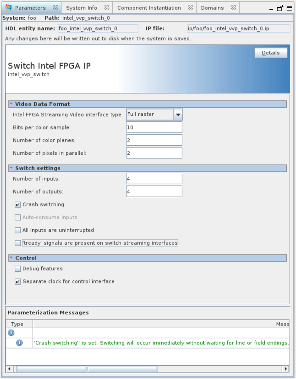
41.2. Switch IP Parameters
The IP offers compile- and run-time parameters.
| Parameter | Values | Description |
|---|---|---|
| Video Data Format | ||
| Intel FPGA streaming video interface type | Full, Lite, Full raster | Select the required streaming video protocol. |
| Bits per color sample | 8 to 16 | Select the number of bits per color sample. |
| Number of color planes | 1 to 4 | Select the number of color planes per pixel. |
| Number of pixels in parallel | 1 to 8 | Select the number of color planes per pixel. |
| Switch settings | ||
| Number of inputs | 1 to 8 | Select the number of inputs required |
| Number of outputs | 1 to 8 | Select the number of outputs required |
| Crash switching | On or off | Select the type of switching required. Crash switching may cut short packets. |
| Autoconsume inputs | On or off | Turn on to allow inputs to consume automatically during switches if required. |
| All inputs are uninterrupted | On or off | For lite variants, turn on only when you can ensure that the start of another field always follows the end of each field. If you turn on for lite variants, the switch occurs at the start-of-field, as indicated by TUSER[0]. If you turn off for lite variants, the IP switch occurs at the end of each line, as indicated by TLAST. Full variants do not use this parameter, as the switch always occurs at field boundaries. |
| ‘tready’ signal present on switch streaming interfaces | On or off | For full raster variants only, select if tready signals are present on the switch inputs and output connections. |
| Control settings | ||
| Debug features | On or off | No effect. The Switch IP has no debugging features. |
| Separate clock for control interface | On or off | Turn on for a separate clock for the control interface |
Figure 109. Switch IP GUI