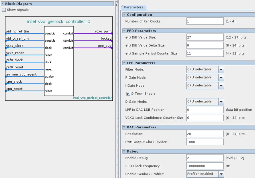
31.2. Genlock Controller IP Parameters
| Parameter | Values | Description |
|---|---|---|
| Configuration | ||
| Number of reference clock | 1 to 4 | The number of reference clocks as source for VCXO tracking. |
| PFD Parameters | ||
| Differential value size | 12 to 27 | The size of the PFD clock counters and output difference value. |
| Differential value size | 8 to 24 | The number of bits for the error counter to calculate the difference between two samples of output difference values. |
| Sample period counter size | 4 to 32 | Select how many least significant bits (LSB) the IP uses for the sample period counter. |
| LPF Parameters | ||
| Filter Mode | Frequency Mode Phase Mode CPU selectable |
Select the filter mode |
| P Gain Mode | Positive Only Negative Only CPU selectable |
Select the proportional gain modes |
| I Gain Mode | Positive Only Negative Only CPU selectable |
Select the integral gain modes |
| D Term enable | On or off | Turn on the derivative term logic |
| D Gain Mode | Positive Only Negative Only CPU selectable |
Select the derivative gain modes. |
| LPF to DAC LSB Position | 0 to 3 | Select the LPF output to DAC least significant bit position. Allows the IP to ignore error wobble by moving the LSB. |
| VCXO Lock Confidence Counter Size | 6 to 32 | The lock confidence count size in bits. The number of successive samples with no error before the IP indicates lock. |
| DAC Parameters | ||
| Resolution | 8 to 24 | PWM DAC value output size. Defines the precision of the value to drive the DAC. Higher number of bits indicates more resolution, and longer time to lock. Fewer bits could decrease the locking time but increase the VCXO jitter. |
| PMW Output Clock Divider | 3 to 4096 | The IP divides the VCXO clock by this value (and then by an additional 2). The IP uses the value to drive the DAC output pin. The value should be low enough to provide a fast response, but not too low to increase VCXO jitter. |
| Debug | ||
| Enable Debug | 0 to 2 | Extra CPU debugging registers:
|
| Enable Genlock Profiler | Profiler enabled Profiler disabled |
The profiler allows you to measure the difference between receive and transmit video pixel clocks. The profiler also measures the latency between receive and transmit start-of-frame (SOF) toggle signals. |
| CPU Clock Frequency | 1 MHz to 1 GHz | CPU clock frequency for measuring VCXO and reference clock frequencies for debugging, |