Video and Vision Processing Suite Intel® FPGA IP User Guide

ID 683329
Date 4/01/2024
Public
Document Table of Contents
1. About the Video and Vision Processing Suite 2. Getting Started with the Video and Vision Processing IPs 3. Video and Vision Processing IPs Functional Description 4. Video and Vision Processing IP Interfaces 5. Video and Vision Processing IP Registers 6. Video and Vision Processing IPs Software Programming Model 7. Protocol Converter Intel® FPGA IP 8. 1D LUT Intel® FPGA IP 9. 3D LUT Intel® FPGA IP 10. AXI-Stream Broadcaster Intel® FPGA IP 11. Bits per Color Sample Adapter Intel FPGA IP 12. Black Level Correction Intel® FPGA IP 13. Black Level Statistics Intel® FPGA IP 14. Chroma Key Intel® FPGA IP 15. Chroma Resampler Intel® FPGA IP 16. Clipper Intel® FPGA IP 17. Clocked Video Input Intel® FPGA IP 18. Clocked Video to Full-Raster Converter Intel® FPGA IP 19. Clocked Video Output Intel® FPGA IP 20. Color Plane Manager Intel® FPGA IP 21. Color Space Converter Intel® FPGA IP 22. Defective Pixel Correction Intel® FPGA IP 23. Deinterlacer Intel® FPGA IP 24. Demosaic Intel® FPGA IP 25. FIR Filter Intel® FPGA IP 26. Frame Cleaner Intel® FPGA IP 27. Full-Raster to Clocked Video Converter Intel® FPGA IP 28. Full-Raster to Streaming Converter Intel® FPGA IP 29. Genlock Controller Intel® FPGA IP 30. Generic Crosspoint Intel® FPGA IP 31. Genlock Signal Router Intel® FPGA IP 32. Guard Bands Intel® FPGA IP 33. Histogram Statistics Intel® FPGA IP 34. Interlacer Intel® FPGA IP 35. Mixer Intel® FPGA IP 36. Pixels in Parallel Converter Intel® FPGA IP 37. Scaler Intel® FPGA IP 38. Stream Cleaner Intel® FPGA IP 39. Switch Intel® FPGA IP 40. Tone Mapping Operator Intel® FPGA IP 41. Test Pattern Generator Intel® FPGA IP 42. Unsharp Mask Intel® FPGA IP 43. Video and Vision Monitor Intel FPGA IP 44. Video Frame Buffer Intel® FPGA IP 45. Video Frame Reader Intel FPGA IP 46. Video Frame Writer Intel FPGA IP 47. Video Streaming FIFO Intel® FPGA IP 48. Video Timing Generator Intel® FPGA IP 49. Vignette Correction Intel® FPGA IP 50. Warp Intel® FPGA IP 51. White Balance Correction Intel® FPGA IP 52. White Balance Statistics Intel® FPGA IP 53. Design Security 54. Document Revision History for Video and Vision Processing Suite User Guide

17.1. About the Clocked Video Input IP

The Clocked Video Input IP allows transferring video data between a timing-aware clocked video input interface and a timing-agnostic video streaming output interface. The IP provides a seamless conversion by removing video timing data from a full-raster bus and leaves just the pixel data in Intel FPGA streaming video format. Typically, the IP is a bridge to transfer data from video connectivity to video processing IP.
The IP accepts full-raster video input format as a full-raster interface of pixel data and timing markers embedded in the TDATA bus of an AXI4-S interface. Also, the IP filters out the timing markers from the TDATA bus and provides a video-active only data format on the output interfaces that conforms to the Intel FPGA streaming video protocol specification.
Figure 31. Clocked Video Input IP Block Diagram

The IP provides a wide variety of video statistic collection, e.g. frame counter, frame per second, active and blanking video frame information. All this information is accessible directly from a processor register interface.

Figure 32. Video Statistics Information

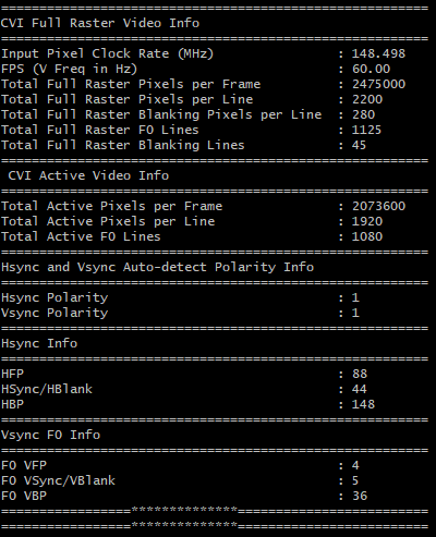
The figure provides an example of the video statistics information that the IP can provide for a 1080p60 video resolution.

By default, the IP only provides full-raster and video active high and width information as part of the video statistic collection. However, if you select the video telemetrics information in the GUI, the IP provides a more comprehensive set of video timing parameters. An optional frame per second counter provides you with an accurate frame rate estimation and its corresponding full-raster video clock.

The IP provides autopolarity detection for the horizontal and vertical timing markers, Vsynch and Hsynch, and allows automatic detection of interlaced video formats. You can configure automatic detection using the processor control interface.

Figure 33. Full-Raster TimingThe figure shows how the video statistics values collected by the IP correlate with a full-raster video frame.

The IP also provides an asynchronous FIFO buffer to handle the clock domain jump from input to output video domain. An optional frame cleaner is available at the back end of the IP. The frame cleaner allows you to automatically pad an incomplete frame (for example, because of an unplugged cable) by inserting a user configurable color pattern. You can turn on or off the frame cleaner at run time using the processor control interface.

Figure 34. Corrupted FrameThe figure shows an example where an output frame is corrupted, and the embedded frame cleaner adds padding (pink pixels) from the Clocked Video Input IP to complete the video output raster.