External Memory Interfaces Intel® Agilex™ FPGA IP User Guide
A newer version of this document is available. Customers should click here to go to the newest version.
3.3.4.2.1. QDR-IV Read Calibration
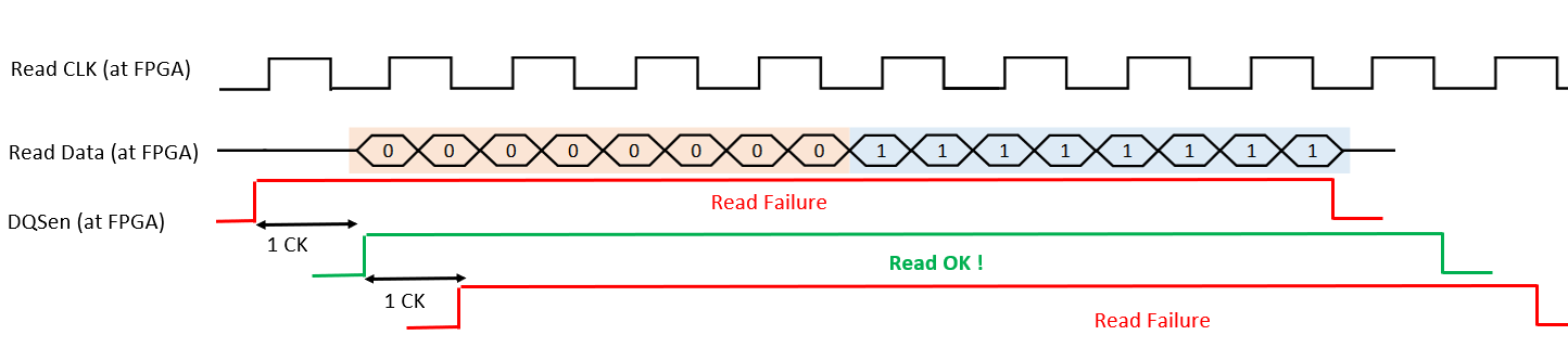
DQSen Calibration
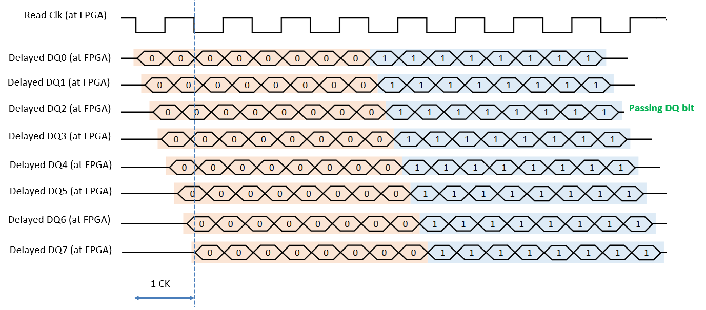
The calibration algorithm does not use a hardware state machine; rather, it calibrates cycle-level delays using software, and subcycle delays using DQS tracking hardware. The algorithm requires good data in memory, and therefore relies on guaranteed writes. The algorithm enables DQS tracking to calibrate the phase component of DQS enable, and then issues a guaranteed write, followed by back-to-back reads. The algorithm sweeps DQSen values cycle by cycle until the read operation succeeds. Because the DQSen calibration occurs before Read Deskew, only one successful data bit is required to register a pass. The algorithm staggers the read DQ bus to ensure that at least one DQ bit falls within the valid Read window.The process then repeats for all other read groups.
Deskew Calibration
Read deskew calibration occurs before write leveling, and must occur at least twice: once before write calibration using simple data patterns from guaranteed writes, and again after write calibration using complex data patterns.
To ensure that guaranteed writes work correctly, the Write Leveling Phase training occurs before the guaranteed writes. The goal of Write Leveling Phase training is to align the rising edge for write DQS with the rising edge of MEM_CLK at the DRAM.

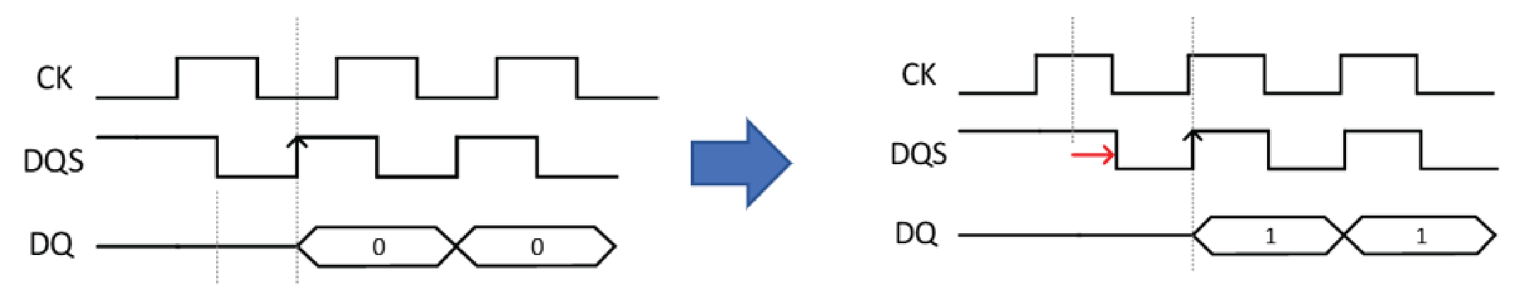
The algorithm uses the DRAM write leveling feature for Write Leveling Phase Training. In this mode the following actions occur:
- The algorithm adjusts the DQS output delay (at the FPGA side) while toggling write DQS signal.
- The DRAM samples the MEM_CLK using the rising edge of write DQS and outputs the sampled value on DQ pins.
- The algorithm continues to adjust the DQS output while toggling the write_DQS signal until it detects a 0 to 1 transition on the DQ pins.
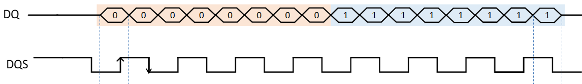
In guaranteed writes, the algorithm writes a burst of 0s to one location and a burst of 1s to another location. The data from the back-to back reads from these two locations is used as a simple data pattern for read deskew calibration.

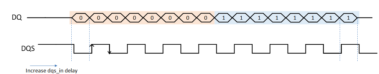
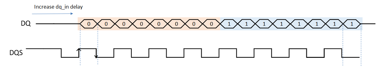
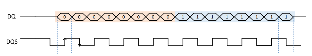
Before the write calibration, the deskew calibration algorithm performs a guaranteed write, and then sweeps dqs_in delay values from low to high, to find the right-hand edge of the read window. The algorithm then sweeps dq_in delay values from low to high, to find the left-hand edge of the read window. The algorithm then applies updated dqs_in and dq_in delay values to center the read window. The process then repeats for all data pins.
After the write path is calibrated, the algorithm performs another read-deskew calibration using a complex data pattern.
Vref-in Calibration
Read LFIFO calibration normalizes read delays between groups. The PHY must present all data to the controller as a single data bus. The LFIFO latency should be large enough for the slowest read data group, and large enough to allow proper synchronization across FIFOs.
LFIFO Calibration
Read LFIFO calibration normalizes read delays between groups. The PHY must present all data to the controller as a single data bus. The LFIFO latency should be large enough for the slowest read data group, and large enough to allow proper synchronization across FIFOs.