Visible to Intel only — GUID: aec1572136912881
Ixiasoft
1. About the External Memory Interfaces Intel® Agilex™ FPGA IP
2. Intel® Agilex™ FPGA EMIF IP – Introduction
3. Intel® Agilex™ FPGA EMIF IP – Product Architecture
4. Intel® Agilex™ FPGA EMIF IP – End-User Signals
5. Intel® Agilex™ FPGA EMIF IP – Simulating Memory IP
6. Intel® Agilex™ FPGA EMIF IP – DDR4 Support
7. Intel® Agilex™ FPGA EMIF IP – QDR-IV Support
8. Intel® Agilex™ FPGA EMIF IP – Timing Closure
9. Intel® Agilex™ FPGA EMIF IP – I/O Timing Closure
10. Intel® Agilex™ FPGA EMIF IP – Controller Optimization
11. Intel® Agilex™ FPGA EMIF IP – Debugging
12. External Memory Interfaces Intel® Agilex™ FPGA IP User Guide Archives
13. Document Revision History for External Memory Interfaces Intel® Agilex™ FPGA IP User Guide
3.1. Intel® Agilex™ EMIF Architecture: Introduction
3.2. Intel® Agilex™ EMIF Sequencer
3.3. Intel® Agilex™ EMIF Calibration
3.4. Intel® Agilex™ EMIF Controller
3.5. User-requested Reset in Intel® Agilex™ EMIF IP
3.6. Intel® Agilex™ EMIF for Hard Processor Subsystem
3.7. Using a Custom Controller with the Hard PHY
3.1.1. Intel® Agilex™ EMIF Architecture: I/O Subsystem
3.1.2. Intel® Agilex™ EMIF Architecture: I/O SSM
3.1.3. Intel® Agilex™ EMIF Architecture: I/O Bank
3.1.4. Intel® Agilex™ EMIF Architecture: I/O Lane
3.1.5. Intel® Agilex™ EMIF Architecture: Input DQS Clock Tree
3.1.6. Intel® Agilex™ EMIF Architecture: PHY Clock Tree
3.1.7. Intel® Agilex™ EMIF Architecture: PLL Reference Clock Networks
3.1.8. Intel® Agilex™ EMIF Architecture: Clock Phase Alignment
3.3.4.3.1. Debugging Calibration Failure Using Information from the Calibration report
3.3.4.3.2. Debugging Address and Command Leveling Calibration Failure
3.3.4.3.3. Debugging Address and Command Deskew Failure
3.3.4.3.4. Debugging DQS Enable Failure
3.3.4.3.5. Debugging Read Deskew Calibration Failure
3.3.4.3.6. Debugging VREFIN Calibration Failure
3.3.4.3.7. Debugging LFIFO Calibration Failure
3.3.4.3.8. Debugging Write Leveling Failure
3.3.4.3.9. Debugging Write Deskew Calibration Failure
3.3.4.3.10. Debugging VREFOUT Calibration Failure
4.1.1.1. local_reset_req for DDR4
4.1.1.2. local_reset_status for DDR4
4.1.1.3. pll_ref_clk for DDR4
4.1.1.4. pll_locked for DDR4
4.1.1.5. ac_parity_err for DDR4
4.1.1.6. oct for DDR4
4.1.1.7. mem for DDR4
4.1.1.8. status for DDR4
4.1.1.9. afi_reset_n for DDR4
4.1.1.10. afi_clk for DDR4
4.1.1.11. afi_half_clk for DDR4
4.1.1.12. afi for DDR4
4.1.1.13. emif_usr_reset_n for DDR4
4.1.1.14. emif_usr_clk for DDR4
4.1.1.15. ctrl_amm for DDR4
4.1.1.16. ctrl_amm_aux for DDR4
4.1.1.17. ctrl_auto_precharge for DDR4
4.1.1.18. ctrl_user_priority for DDR4
4.1.1.19. ctrl_ecc_user_interrupt for DDR4
4.1.1.20. ctrl_ecc_readdataerror for DDR4
4.1.1.21. ctrl_ecc_status for DDR4
4.1.1.22. ctrl_mmr_slave for DDR4
4.1.1.23. hps_emif for DDR4
4.1.1.24. emif_calbus for DDR4
4.1.1.25. emif_calbus_clk for DDR4
4.1.2.1. local_reset_req for QDR-IV
4.1.2.2. local_reset_status for QDR-IV
4.1.2.3. pll_ref_clk for QDR-IV
4.1.2.4. pll_locked for QDR-IV
4.1.2.5. oct for QDR-IV
4.1.2.6. mem for QDR-IV
4.1.2.7. status for QDR-IV
4.1.2.8. afi_reset_n for QDR-IV
4.1.2.9. afi_clk for QDR-IV
4.1.2.10. afi_half_clk for QDR-IV
4.1.2.11. afi for QDR-IV
4.1.2.12. emif_usr_reset_n for QDR-IV
4.1.2.13. emif_usr_clk for QDR-IV
4.1.2.14. ctrl_amm for QDR-IV
4.1.2.15. emif_calbus for QDR-IV
4.1.2.16. emif_calbus_clk for QDR-IV
4.4.1. ctrlcfg0
4.4.2. ctrlcfg1
4.4.3. dramtiming0
4.4.4. sbcfg1
4.4.5. caltiming0
4.4.6. caltiming1
4.4.7. caltiming2
4.4.8. caltiming3
4.4.9. caltiming4
4.4.10. caltiming9
4.4.11. dramaddrw
4.4.12. sideband0
4.4.13. sideband1
4.4.14. sideband4
4.4.15. sideband6
4.4.16. sideband7
4.4.17. sideband9
4.4.18. sideband11
4.4.19. sideband12
4.4.20. sideband13
4.4.21. sideband14
4.4.22. dramsts
4.4.23. niosreserve0
4.4.24. niosreserve1
4.4.25. sideband16
4.4.26. ecc3: ECC Error and Interrupt Configuration
4.4.27. ecc4: Status and Error Information
4.4.28. ecc5: Address of Most Recent SBE/DBE
4.4.29. ecc6: Address of Most Recent Correction Command Dropped
4.4.30. ecc7: Extension for Address of Most Recent SBE/DBE
4.4.31. ecc8: Extension for Address of Most Recent Correction Command Dropped
6.1.1. Intel Agilex EMIF IP DDR4 Parameters: General
6.1.2. Intel Agilex EMIF IP DDR4 Parameters: Memory
6.1.3. Intel Agilex EMIF IP DDR4 Parameters: Mem I/O
6.1.4. Intel Agilex EMIF IP DDR4 Parameters: FPGA I/O
6.1.5. Intel Agilex EMIF IP DDR4 Parameters: Mem Timing
6.1.6. Intel Agilex EMIF IP DDR4 Parameters: Controller
6.1.7. Intel Agilex EMIF IP DDR4 Parameters: Diagnostics
6.1.8. Intel Agilex EMIF IP DDR4 Parameters: Example Designs
6.5.1. Terminations for DDR4 with Intel® Agilex™ Devices
6.5.2. Clamshell Topology
6.5.3. General Layout Routing Guidelines
6.5.4. Reference Stackup
6.5.5. Intel® Agilex™ EMIF-Specific Routing Guidelines for Various DDR4 Topologies
6.5.6. DDR4 Routing Guidelines: Discrete (Component) Topologies
6.5.7. Intel® Agilex™ EMIF Pin Swapping Guidelines
6.5.5.1. One DIMM per Channel (1DPC) for UDIMM, RDIMM, LRDIMM, and SODIMM DDR4 Topologies
6.5.5.2. Two DIMMs per Channel (2DPC) for UDIMM, RDIMM, and LRDIMM DDR4 Topologies
6.5.5.3. Two DIMMs per Channel (2DPC) for SODIMM Topology
6.5.5.4. Skew Matching Guidelines for DIMM Configurations
6.5.5.5. Power Delivery Recommendations for the Memory / DIMM Side
6.5.6.1. Single Rank x 8 Discrete (Component) Topology
6.5.6.2. Single Rank x 16 Discrete (Component) Topology
6.5.6.3. ADDR/CMD Reference Voltage/RESET Signal Routing Guidelines for Single Rank x 8 and R Rank x 16 Discrete (Component) Topologies
6.5.6.4. Skew Matching Guidelines for DDR4 Discrete Configurations
6.5.6.5. Power Delivery Recommendations for DDR4 Discrete Configurations
7.1.1. Intel Agilex EMIF IP QDR-IV Parameters: General
7.1.2. Intel Agilex EMIF IP QDR-IV Parameters: Memory
7.1.3. Intel Agilex EMIF IP QDR-IV Parameters: FPGA I/O
7.1.4. Intel Agilex EMIF IP QDR-IV Parameters: Mem Timing
7.1.5. Intel Agilex EMIF IP QDR-IV Parameters: Controller
7.1.6. Intel Agilex EMIF IP QDR-IV Parameters: Diagnostics
7.1.7. Intel Agilex EMIF IP QDR-IV Parameters: Example Designs
7.3.3.1. Intel® Agilex™ FPGA EMIF IP Banks
7.3.3.2. General Guidelines
7.3.3.3. QDR IV SRAM Commands and Addresses, AP, and AINV Signals
7.3.3.4. QDR IV SRAM Clock Signals
7.3.3.5. QDR IV SRAM Data, DINV, and QVLD Signals
7.3.3.6. Specific Pin Connection Requirements
7.3.3.7. Resource Sharing Guidelines (Multiple Interfaces)
9.1. I/O Timing Closure Overview
9.2. Collateral Generated with Your EMIF IP
9.3. SPICE Decks
9.4. File Organization
9.5. Top-level Parameterization File
9.6. IP-Supplied Parameters that You Might Need to Override
9.7. Understanding the *_ip_parameters.dat File and Making a Mask Polygon
9.8. Multi-Rank Topology
9.9. Pin Parasitics
9.10. Mask Evaluation
10.4.1. Auto-Precharge Commands
10.4.2. Additive Latency
10.4.3. Bank Interleaving
10.4.4. Additive Latency and Bank Interleaving
10.4.5. User-Controlled Refresh
10.4.6. Frequency of Operation
10.4.7. Series of Reads or Writes
10.4.8. Data Reordering
10.4.9. Starvation Control
10.4.10. Command Reordering
10.4.11. Bandwidth
10.4.12. Enable Command Priority Control
10.4.13. Controller Pre-pay and Post-pay Refresh (DDR4 Only)
11.1. Interface Configuration Performance Issues
11.2. Functional Issue Evaluation
11.3. Timing Issue Characteristics
11.4. Verifying Memory IP Using the Signal Tap Logic Analyzer
11.5. Hardware Debugging Guidelines
11.6. Categorizing Hardware Issues
11.7. Debugging with the External Memory Interface Debug Toolkit
11.8. Using the Default Traffic Generator
11.9. Using the Configurable Traffic Generator (TG2)
11.10. EMIF On-Chip Debug Port
11.11. Efficiency Monitor
11.5.1. Create a Simplified Design that Demonstrates the Same Issue
11.5.2. Measure Power Distribution Network
11.5.3. Measure Signal Integrity and Setup and Hold Margin
11.5.4. Vary Voltage
11.5.5. Operate at a Lower Speed
11.5.6. Determine Whether the Issue Exists in Previous Versions of Software
11.5.7. Determine Whether the Issue Exists in the Current Version of Software
11.5.8. Try A Different PCB
11.5.9. Try Other Configurations
11.5.10. Debugging Checklist
11.7.4.3.1. Debugging Calibration Failure Using Information from the Calibration report
11.7.4.3.2. Debugging Address and Command Leveling Calibration Failure
11.7.4.3.3. Debugging Address and Command Deskew Failure
11.7.4.3.4. Debugging DQS Enable Failure
11.7.4.3.5. Debugging Read Deskew Calibration Failure
11.7.4.3.6. Debugging VREFIN Calibration Failure
11.7.4.3.7. Debugging LFIFO Calibration Failure
11.7.4.3.8. Debugging Write Leveling Failure
11.7.4.3.9. Debugging Write Deskew Calibration Failure
11.7.4.3.10. Debugging VREFOUT Calibration Failure
11.9.1. Enabling the Traffic Generator in a Design Example
11.9.2. Traffic Generator Block Description
11.9.3. Default Traffic Pattern
11.9.4. Configuration and Status Registers
11.9.5. User Pattern
11.9.6. Traffic Generator Status
11.9.7. Starting Traffic with the Traffic Generator
11.9.8. Traffic Generator Configuration User Interface
Visible to Intel only — GUID: aec1572136912881
Ixiasoft
6.5.6.3. ADDR/CMD Reference Voltage/RESET Signal Routing Guidelines for Single Rank x 8 and R Rank x 16 Discrete (Component) Topologies
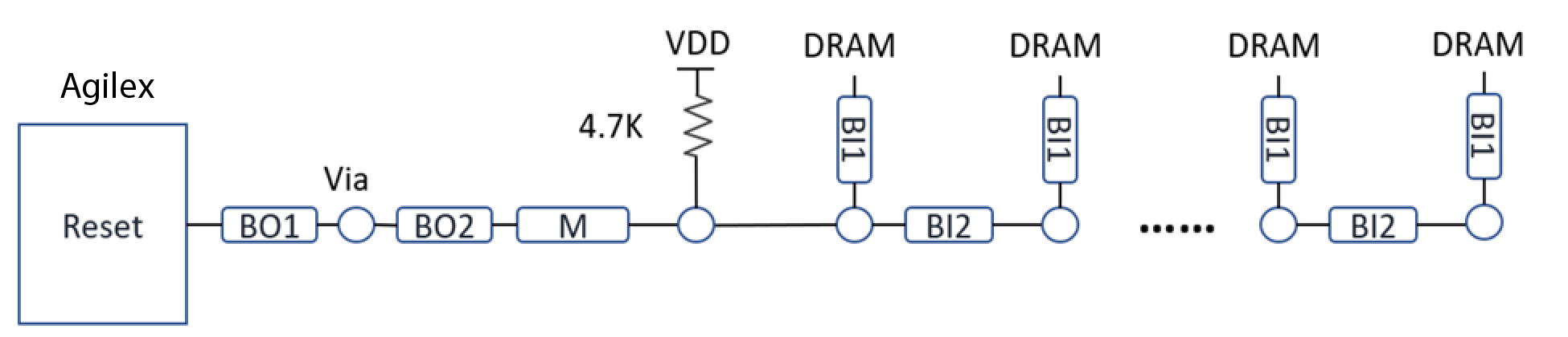
The target impedance for the RESET signal is 50 ohms. The RESET signal must have at least 3 × h (where h is the distance from the trace to the nearest reference plane) spacing to other nearby signals on the same layer. The end-to-end RESET trace length is not limited but must not exceed 5 inches to the first DRAM.
The following figure shows the RESET routing scheme, which you can apply to both single rank x 8 and single rank x16 topologies.
Figure 110. RESET Scheme for Single Rank x8 and Single Rank x16 Topologies
The Address/Command reference voltage input (VREF_CA) must track the VTT regulator output as closely as possible. There are two methods to achieve this:
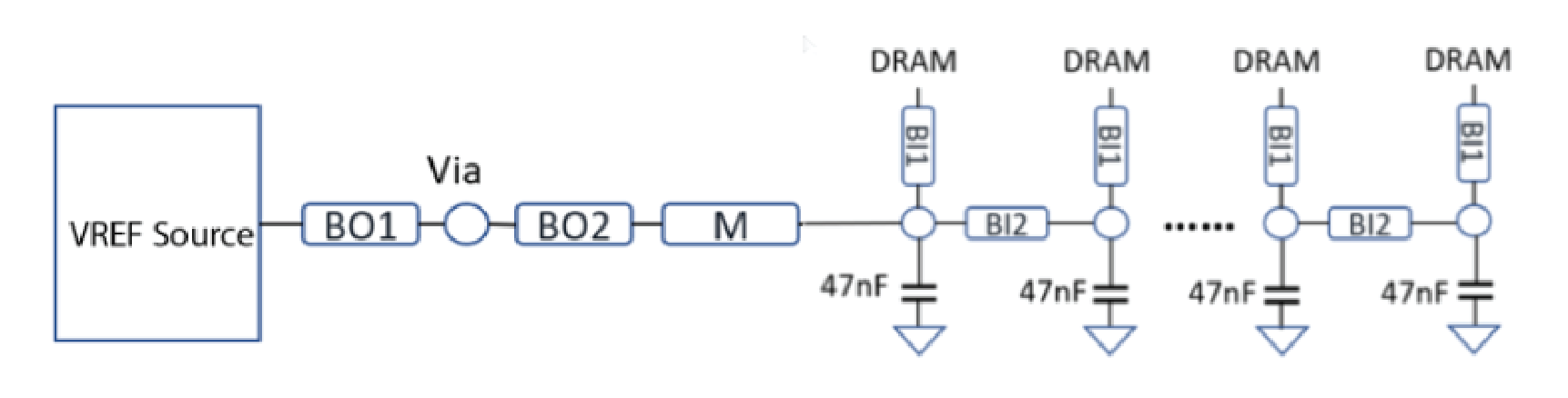
One method is to use a regulator that provides a dedicated tracking voltage reference output that can be connected directly to memory component VREF_CA inputs, as shown in the figure below.
Figure 112. VTT Regulator Supplies VREF_CA Output
A second method is to create a voltage divider using precision resistors. Place the resistor network in a location that is likely to track IR losses on the VDD supply due to memory loading (that is, close to the VTT regulator or memory components, rather than next to the VDD regulator output). The following figure illustrates this configuration.
Figure 113. Resistor Divider Provides the VREF_CA Signal
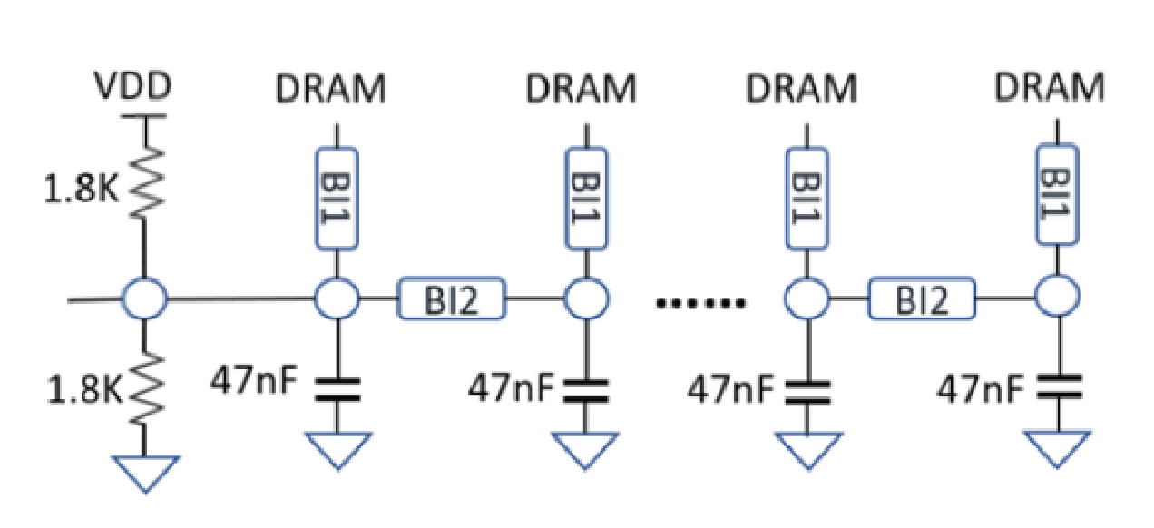
Intel® recommends using a PCB trace width of at least 10 mils for VREF_CA routing. The VREF_CA signal must have at least 3×h spacing (where h is the distance or height from the trace to the nearest reference plane) to other nearby signals on the same layer.