External Memory Interfaces Intel® Agilex™ FPGA IP User Guide
A newer version of this document is available. Customers should click here to go to the newest version.
6.4.3.1. Intel® Agilex™ FPGA EMIF IP Banks
The following diagram illustrates a typical Intel® Agilex™ FPGA with all banks bonded out to pins.
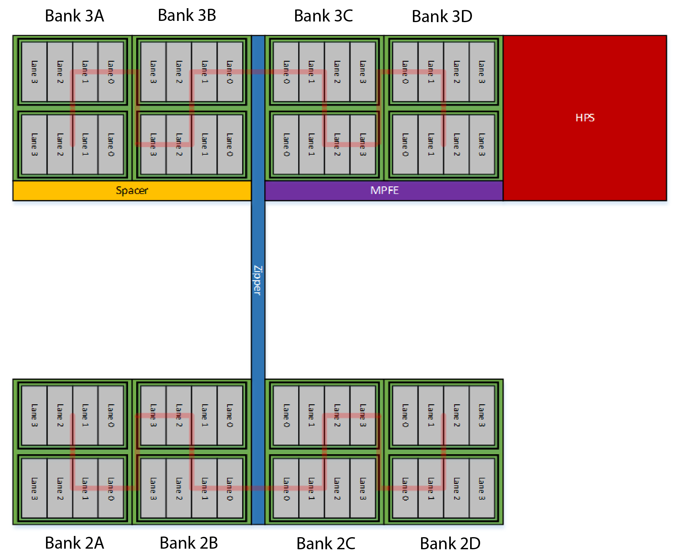
In the above diagram, the group of 4 lanes in the top-left corner (the top sub-bank in bank 3A), denotes the IO48 block that is used for test mode and AVST configuration. If all I/O lanes in this sub-bank are used for configuration, then this bank cannot be used for the external memory interface. Similarly, the bottom sub-bank in bank 3A could not be used for the external memory interface either, because all the I/O sub-banks in a given interface must be contiguous.
The red line in the above diagram denotes the chaining order of the sub-banks to form an external memory interface. The chaining order flips when crossing the zipper.
For additional details, refer to the Intel® Agilex™ FPGA EMIF IP Product Architecture chapter.