External Memory Interfaces Intel® Agilex™ FPGA IP User Guide
A newer version of this document is available. Customers should click here to go to the newest version.
6.5.5.2. Two DIMMs per Channel (2DPC) for UDIMM, RDIMM, and LRDIMM DDR4 Topologies
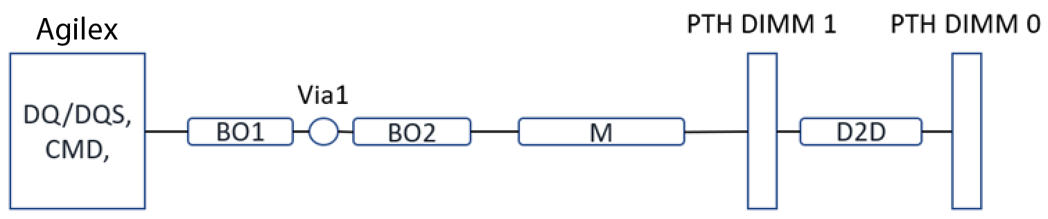
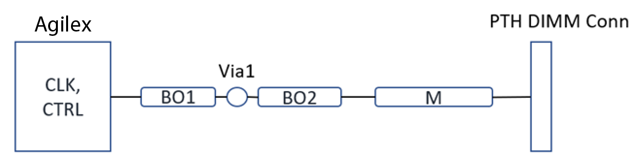
The following figure illustrates the signal connection topology for a PTH type of connector for UDIMM, RDIMM, and LRDIMM topologies.
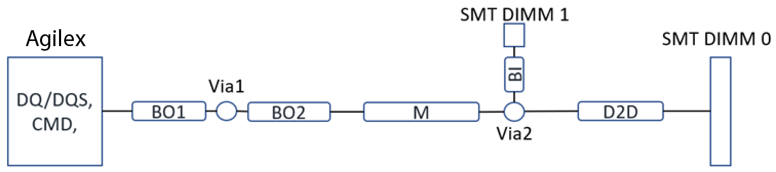
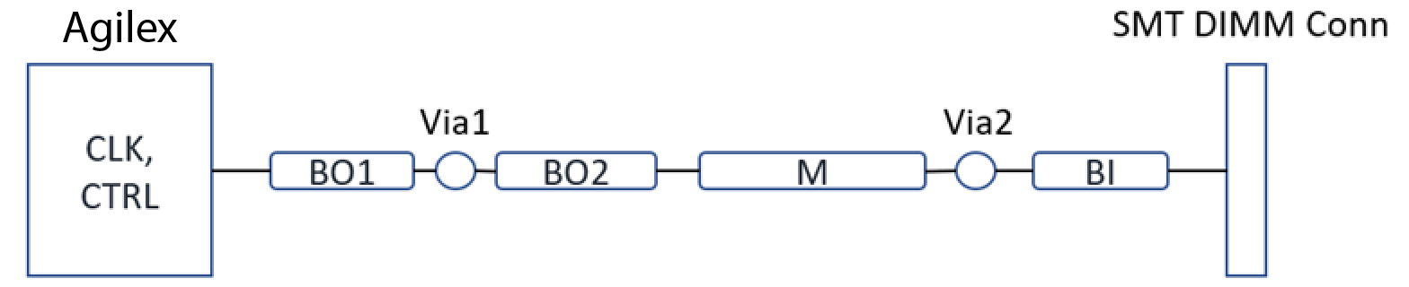
The following figure illustrates the signal connection topology for an SMT type of connector for UDIMM, RDIMM, and LRDIMM topologies.
The following table provides specific routing guidelines for two DIMMs per channel in UDIMM, RDIMM, LRDIMM, and SODIMM topologies for all supported signals in the interface.
| Signal Group | Segment | Routing Layer | Max Length (mil) | Target Zse (ohm) | Trace Width, W (mil) | Trace Spacing, S1 (mil): Within Group | Trace Spacing, S2 (mil): CMD/CTRL/CLK to DQ/DQS | Trace Spacing, S3 (mil):DQ Nibble to Nibble | Trace Spacing (mil), Within DIFF Pair | Trace Spacing (mil), DQS pair to DQ | Trace Spacing (mil), CLK pair to CMD/CTRL/CKE | Channel to Channel Spacing (DQ to DQ between two channels) | |
|---|---|---|---|---|---|---|---|---|---|---|---|---|---|
| Segment | Total MB | ||||||||||||
| CLK | BO1 | US | 50 | 5000 | 4 | 5, 17 | 5, 17 | 4 | 17 | ||||
| BO2 | SL | 1000 | 4 | 5, 17 | 5, 17 | 4 | 17 | ||||||
| M | SL | 45 | 4.5 | 12 (3h) | 4 | 12 (3h) | |||||||
| BI | US | 50 | 4 | 12 (3h) | 4 | 12 (3h) | |||||||
| CMD, ALERT | BO1 | US | 50 | 5000 | 4 | 5, 17 | 5, 17 | ||||||
| BO2 | SL | 1000 | 4 | 5, 17 | 5, 17 | ||||||||
| M | SL | 40 | 5.5 | 8 (2h) | 12 (3h) | ||||||||
| BI | US | 100 | 4 | 8 (2h) | 12 (3h) | ||||||||
| D2D | SL | PTH: 340 SMT: 400 | 5.5 | 8 (2h) | 12 (3h) | ||||||||
| CTRL | BO1 | US | 50 | 5000 | 4 | 5, 17 | 5, 17 | ||||||
| BO2 | SL | 100 | 4 | 5, 17 | 5, 17 | ||||||||
| M | SL | 45 | 4.5 | 8 (2h) | 12 (3h) | ||||||||
| BI | US | 100 | 4 | 12 (3h) | |||||||||
| DQ | BO1 | US | 50 | 5000 | 3 | 5, 17 | 17 | 17 | |||||
| BO2 | SL | 1000 | 3 | 5, 17 | 17 | 17 | |||||||
| M | SL | 40 | 5.5 | 8 (2h) | 12 (3h) | 16 (4h) | |||||||
| BI | US | 50 | 4 | 8 (2h) | 12 (3h) | 16 (4h) | |||||||
| D2D | SL | PTH: 500 SMT: 400 | 4 | 8 (2h) | 12 (3h) | 16 (4h) | |||||||
| DQS | BO1 | US | 50 | 5000 | 3 | 5, 17 | 4 | 17 | |||||
| BO2 | SL | 1000 | 3 | 5, 17 | 4 | 17 | |||||||
| M | SL | 40 | 5.5 | 4 | 12 (3h) | ||||||||
| BI | US | 50 | 4 | ||||||||||
| D2D | SL | PTH: 500 SMT: 400 | 4 | ||||||||||
| For an explanation of the guidelines represented in this table, refer to the bullet points immediately following Figure 99. | |||||||||||||
The following figure shows the RESET signal scheme and routing guideline for two DIMMs per channel topologies.
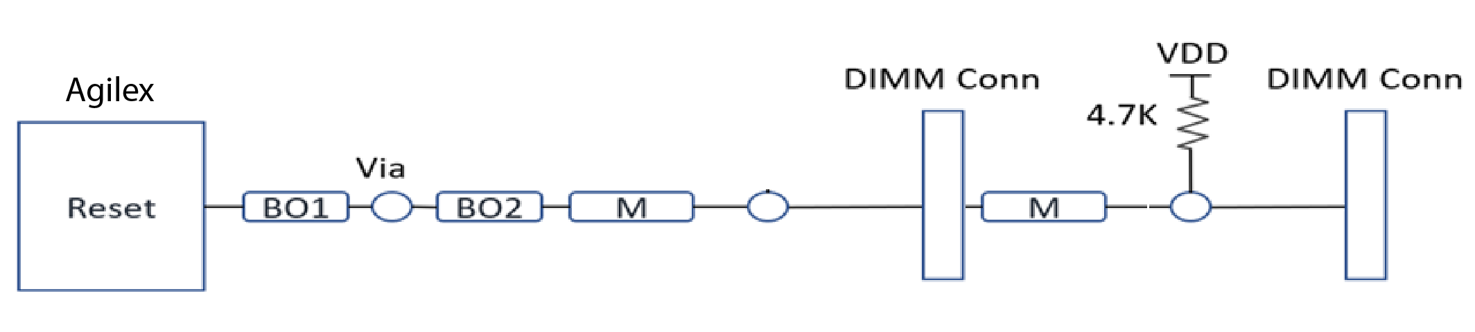
The target impedance for the RESET signal is 50 ohms. The RESET signal shall have at least 3×h (where h stands for trace to nearest reference plane height or distance) spacing to other nearby signals on the same layer. The end-to-end RESET trace length is not limited but shall not exceed 5 inches.