External Memory Interfaces Intel® Agilex™ FPGA IP User Guide
A newer version of this document is available. Customers should click here to go to the newest version.
9.1. I/O Timing Closure Overview
This simulation-based approach for evaluating board signal integrity is new for Intel® Agilex™ devices. With earlier Intel® FPGA families, you had to perform your own simulations to determine signal integrity figures of merit such as crosstalk and ISI, and enter them into the EMIF parameter editor; the channel budget was then calculated as part of the timing analysis performed by the Intel® Quartus® Prime Timing Analyzer.
With the Intel® Agilex™ FPGA EMIF IP, the timing analysis of the external I/O channel is no longer part of the signoff timing analysis flow. The EMIF IP now generates a set of SPICE simulation collateral for evaluating board signal integrity, which you can use in conjunction with extractions from your PCB to generate eye diagrams. The collateral also provides eye masks appropriate to the IP settings and FPGA family that are used to determine if the receiver eye has adequate voltage and timing margin.
Board Signal Integrity Flow
The following steps summarize the high-level tasks comprising the board signal integrity flow:
- Parameterize the EMIF IP to suit your memory interface, and generate the design example to create the board signal integrity (BSI) and synthesis RTL file sets.
- Use the synthesis design example to determine a suitable location for the interface, enabling schematic capture and memory interface PCB layout.
- After you have created an initial layout of the memory interface, PCB extractions are generated in the form of a Touchstone file that captures the multi-port network behavior of the PCB.
- The generated board signal integrity collateral uses these extractions to generate eye diagrams for the address/command path, as well as both data bus write and read operations.
- The SPICE simulation parameters for configuring memory and FPGA IBIS models, as well as appropriate input stimuli to match the IP, are automatically generated for you.
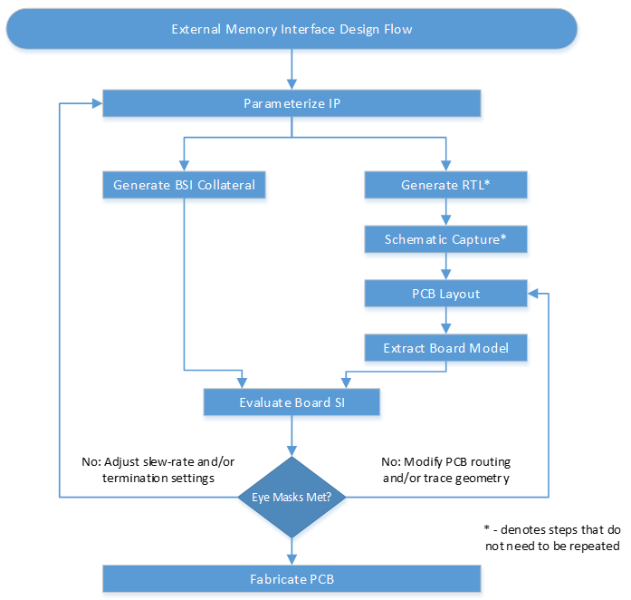
The board signal integrity flow allows you to iterate your design quickly if necessary. You can make adjustments to signal integrity settings such as slew rate, deemphasis, drive strength, or read termination in the parameter editor, and rerun the simulations with the new IP-specific SPICE parameter file. If you cannot achieve mask compliance by modifying the IP, then you can re-route the critical areas of the PCB and repeat the simulation using the updated extracted model.
The following topics in this chapter provide detailed information about the generated SPICE simulation collateral, changes and customizations that you may have to make, as well as guidance for evaluating the generated eye diagrams.