External Memory Interfaces Intel® Agilex™ FPGA IP User Guide
A newer version of this document is available. Customers should click here to go to the newest version.
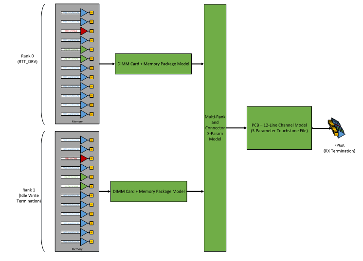
9.3.3. FPGA Read Operation Simulation Deck
The figure below illustrates the composition of the FPGA Read SPICE simulation deck. The composition of the FPGA Read simulation deck is identical to that of the FPGA Write simulation deck, except that the active memory rank serves as the driver and the FPGA is a receiver. The top-level parameterization file configures all electrical settings to match the options for RTT_WR and OCT_IN chosen during IP configuration.
The simulation deck generates an edge-aligned strobe pattern to model the behavior of the DQS pair in a conventional read operation. Similar to the FPGA Write simulation deck, Pin 2 within the lane is a victim pin and driven with a repeating PRBS-10 pattern, and all other DQ and Read DBI pins (if applicable) are aggressors and driven with a PRBS-15 pattern.