External Memory Interfaces Intel® Agilex™ FPGA IP User Guide
A newer version of this document is available. Customers should click here to go to the newest version.
9.3.2. FPGA Write Operation Simulation Deck
For DDR4 interfaces, the 12-line extraction maps either to one x8 DQS group (8 DQ pins, a complementary DQS pair, and a write DBI/DM pin if specified in the IP), or two x4 DQS groups (8 DQ pins and two complementary DQS pairs). The following figure illustrates the composition of the FPGA write SPICE simulation deck.
The simulation deck generates a strobe pattern to model the behavior of the DQS pair in a conventional write operation. Pin 2 within the lane is designated as a victim pin and driven with a repeating PRBS-10 pattern, and all other DQ and DM/DBI pins are designated as aggressors and driven with a PRBS-15 pattern.
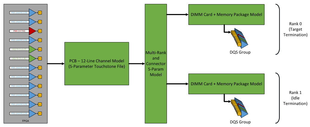
FPGA
At the left side of the above diagram, 12 FPGA IBIS models are instantiated and configured to match the IP-specified DQ and DQS electrical settings. The pattern generators are embedded within this sub-circuit and automatically configured by the IP-generated parameter file.
PCB – 12-Line Channel Model
This block models a 12-line (24-port plus ground) channel that matches the signals implementing any of the DQS groups of the memory interface. For DDR4, this can be either the signals comprising a DQSx8 group (data, DM/DBI and strobes) or two DQSx4 nibbles packed within a single 12-pin lane. Typically, the lane expected to have the worst-case signal integrity should be used for these simulations, however you can run this simulation with models for every lane in the system if you want.
By default, this subcircuit instantiates 12 independent ideal 50-ohm transmission lines, which you can replace with a Touchstone extraction by specifying the following options in the IP-generated parameter file:
| Parameter Name | Default Value | Description |
|---|---|---|
| USE_DQ_PCB_EXTRACTION | False | Specifies whether a 24-port Touchstone extraction is to be used in the FPGA read/write simulation. If set to true, then the DQ_PCB_EXTRACTION_FILE parameter must specify a valid Touchstone file location. If set to false, ideal transmission line models are used |
| DQ_PCB_EXTRACTION_FILE | <empty> | Specifies the file name for the 24-port Touchstone extraction file (.s24p) that represents the data channel. The first 12 pins map to Pins 0 through 11 connected to the balls of the FPGA for the selected DQS group. The next 12 pins map to the far-end of the channel, which is either the memory balls (for direct point-to-point connections) or to the bifurcation point for a multi-rank topology. |
Multi-Rank and Connector Model
Similar to the address/command channel multi-rank/connector model block, you can use this block in cases where you want to do either of the following:
- Model the multi-rank topology of the interface to explore the effect of parameters such as DIMM spacing, channel loading, or component stacking.
- Model the effect of the DIMM connector by inserting a vendor-supplied simulation model.
This block is situated between the end of the DQ PCB extraction model and the start of memory IBIS model receiver bank for each rank. If you do not specify an extraction model, the default model of the block is as follows:
- For single-rank DDR4 systems, the default model for this block is a direct pass-through.
- For dual-rank DDR4 systems, the default model for this block is to connect directly to rank 0, and insert 12 independent 50-ohm, 50ps transmission lines between rank 0 and rank 1 to model a slight delay difference between the two ranks.
- For quad-rank DDR4 systems, the default model for this block is to connect directly to ranks 0 and 1, and insert 12 independent 50-ohm, 50ps transmission lines between ranks 0/1 and ranks 2/3.
You can override this default behavior by specifying an S-Parameter model of your own, using the following options. (Note that the number of ports of the model should align with the IP-calculated value of the number of DQ Ranks in the system, MEM_DQ_RANKS. A value of 1, 2 or 4 correspond to single, dual- or quad-rank systems and require 24, 36 or 60-port models respectively.)
| Parameter Name | Default Value | Description |
|---|---|---|
| USE_DQ_MULTIRANK_CONNECTOR_EXTRACTION | False | Specifies whether a N-port Touchstone extraction is to be used in the FPGA write/read simulation to model the multi-rank bifurcation topology and/or the DIMM connector. If set to true, then the DQ_MULTIRANK_CONNECTOR_EXTRACTION_FILE parameter must specify a valid Touchstone file location. If set to false, ideal transmission line models are used. |
| DQ_MULTIRANK_CONNECTOR_EXTRACTION_FILE | <empty> | Specifies the file name for the N-port Touchstone extraction file (.sNp) that represents the data channel. The first 12 pins map to Lane 0, Pins 0 through 11 connected to the endpoint of the 12-line DQ channel model. The next 12 pins connect to the start of the memory IBIS model receiver bank for Rank 0. If MEM_DQ_RANKS is greater than 1, the next 12 pins connect to the DIMM card/memory package model for Rank 1, and Rank 2 and Rank 3 for quad-rank systems. |