External Memory Interfaces Intel® Agilex™ FPGA IP User Guide
A newer version of this document is available. Customers should click here to go to the newest version.
10.4.4. Additive Latency and Bank Interleaving
The following figure shows an example of bank interleaving in a read operation without additive latency. The example uses bank interleave reads with CAS latency of 5, and burst length of 8.
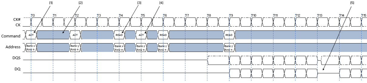
The following sequence of events describes the above figure:
- The controller issues an activate command to open the bank, which activates bank x and the row in it.
- After tRCD time, the controller issues a read with auto-precharge command to the specified bank.
- Bank y receives an activate command after tRRD time.
- The controller cannot issue an activate command to bank z at its optimal location because it must wait for bank x to receive the read with auto‑precharge command, thus delaying the activate command for one clock cycle.
- The delay in activate command causes a gap in the output data from the memory device.
The following figure shows an example of bank interleaving in a read operation with additive latency. The example uses bank interleave reads with additive latency of 3, CAS latency of 5, and burst length of 8. In this configuration, the controller issues back-to-back activate and read with auto-precharge commands.
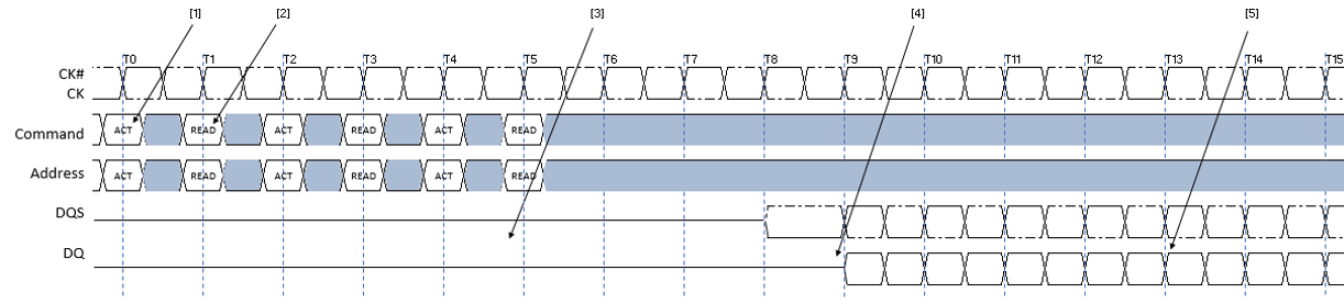
The following sequence of events describes the above figure:
- The controller issues an activate command to bank x.
- The controller issues a read with auto precharge command to bank x right after the activate command, before waiting for the tRCD time.
- The controller executes the read with auto-precharge command tRCD time later on the rising edge T4.
- 5 cycles of CAS latency later, the SDRAM device issues the data on the data bus.
- For burst length of 8, you need 2 cycles for data transfer. Within 2 clocks of giving activate and read with auto-precharge commands, you get a continuous flow of output data.
Compare the efficiency results in the two preceding figures:
- bank interleave reads with no additive latency, CAS latency of 5, and burst length of 8 (first figure),
Number of active cycles of data transfer = 8.
Total number of cycles = 18
Efficiency = 44%
- bank interleave reads with additive latency of 3, CAS latency of 4, and burst length of 4 (second figure),
Number of active cycles of data transfer = 8.
Total number of cycles = 17
Efficiency = approximately 47%
The interleaving reads used with additive latency increases efficiency by approximately 3%.