External Memory Interfaces Intel® Agilex™ FPGA IP User Guide
A newer version of this document is available. Customers should click here to go to the newest version.
3.3.4.2. Calibration Algorithms for QDR-IV
Address and Command Deskew
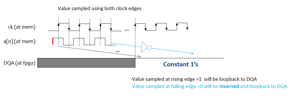
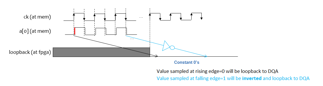
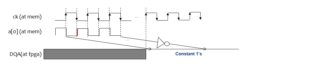
QDR-IV uses the loopback mode for address and command deskew. The FPGA sends address and command signals, and the memory device sends back the address and command signals which it captures, via the read data pin of port A. Each input pin is sampled on both the rising and falling clock edges of input CK/CK#. The output value on the rising edge of output clock QKA/QKA# is the value that was sampled on the rising clock edge of the input clock. The output value on the falling edge of the output clock of QKA/QKA# is the inverted value of what was sampled on the falling edge of the input clock.
By sweeping the output delay on the address and command pins on the FPGA, the algorithm determines the right and left edges of the window, and centers the signal accordingly. Deskew calibration can deskew all synchronous address and command signals,
For more information about loopback mode, refer to your QDR-IV memory device data sheet.