DSP Builder for Intel® FPGAs (Advanced Blockset): Handbook
A newer version of this document is available. Customers should click here to go to the newest version.
7.3.1. DDC Design Example Subsystem
The DDCChip subsystem contains a Device block. This block labels this level of design hierarchy that compiles onto the FPGA. The Device block sets the FPGA family, device and speed grade. The family and speed grade optimize the hardware. In combination with the target clock frequency, the device determines the degree of pipelining.
The DDCChip subsystem has three types of block:
- The grey blocks are IP blocks. These represent functional IP such as black box filters, NCOs, and mixers.
- The blue blocks are processor visible registers.
- The black and white blocks are Simulink blocks.
Figure 47. DDCChip Datapath (NCO and Mixer)
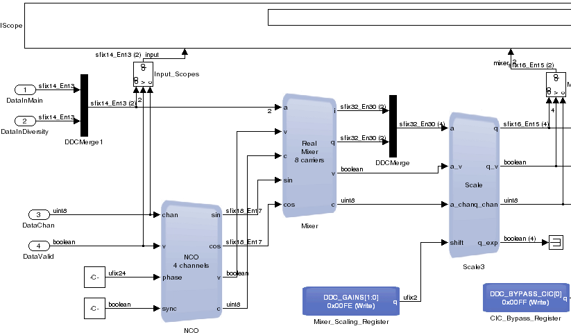
DDCChip Primary Inputs
The primary inputs to the hardware are two parallel data signals (DataInMain and DataInDiversity), a channel signal (DataChan), and a valid signal (DataValid). The parallel data signals represent inputs from two antennas. They are of type sfix14_13 which is a Simulink fixed-point type of total width 14 bits. The type is signed with 13 bits of fraction, which is a typical number format that an analog-to-digital converter generates.
The data channel DataChan is always an 8-bit unsigned integer (uint8) and DSP Builder synthesizes away the top bits if not used. The valid signal DataValid indicates when real data transmits. The first rising edge of the valid signal starts operation of the first blocks in the chain. As the first blocks start producing outputs, their valid outputs start the next blocks in the chain. This mechanism ensures that filter chain start up is coordinated without having a global controller for the latencies of each block. The actual latencies of the blocks may change based on the clock frequency and FPGA selection.
DDC Merge Multiplexer
The IP blockset supports vectors on its input and output data wires, which ensures that a block diagram is scalable when, for example, changing channel counts and operating frequencies. The merge multiplexer (DDCMerge1) takes two individual wires and combines them into a vector wire of width 2. This Simulink Mux block does not perform any multiplexing in hardware—it is just as a vectorizing block. If you examine the RTL, it contains just wires.
DDC NCO
The NCO block generates sine and cosine waveforms to a given precision. These waveforms represent a point in the complex plane rotating around the origin at a given frequency. DSP Builder multiplies this waveform by the incoming data stream to obtain the data from the transmitted signal.
DSP Builder configures the NCO block to produce a signed 18-bit value with 17 bits of fraction. The internal accumulator width is set to 24 bits. This internal precision affects the spurious-free dynamic range (SFDR). DSP Builder specifies the initial frequencies for the simulation as phase increments. The phase accumulator width in bits is 2^24, thus one complete revolution of the unit circle corresponds to a value of 2^24. Dividing this number by 5.95, means that the design requires 5.95 cycles to perform one complete rotation. That is, the wavelength of the sine and cosine that the design produces are 5.95 cycles. The sample rate is 61.44 MHz, therefore the frequency is 61.44/5.95, which is 10.32 MHz.
The input frequency in the testbench rotates every 6 cycles for a frequency of 61.44/6=10.24 MHz. Therefore, you can expect to recover the difference of these frequencies (0.08 MHz or 80 kHz), which fall in the low-pass filters pass bands, because DSP Builder mixes these signals.
The design exposes phase values through a memory-mapped interface at the address specified by the variable DDC_NCO_PHASE_INCR, which is set to address 0x0000 in the setup script. After simulation, to view resource usage for the design example, the subsystem, or a selected block, on the DSP Builder menu, point to Resource Usage and click Design, Current Subsystem, or Selected block.
DSP Builder reports for each register, the name, width, reset value, and address. This report collates all the registers from your design into a single location.
You can view the estimated results for this NCO configuration in the Results tab of the dialog box).
Based on the selected accumulator width and output width, DSP Builder calculates an estimated SFDR and accumulator precision. To verify this precision in a separate testbench, use demo_nco.mdl as a start.
DDC Mixer
The Mixer block performs the superheterodyne operation by multiplying each of the two received signals (DataInMain and DataInDiversity) by each of the four frequencies. This action produces eight complex signals or 16 scalar signals (the 16 channels in the DDC design).
The mixer requires sufficient multipliers to perform this calculation. The total number of real × complex multipliers required for each sample is 2 signals × 4 frequencies = 8.
Thus, 8 real × complex multiplies require 8 × 2 = 16 scalar multipliers. This processing is spread over four cycles (the folding factor given by the ratio of clock rate to sample rate), therefore DSP Builder requires four physical multipliers.
After simulation, to view resource usage for the design example, the subsystem, or a selected block, on the DSP Builder menu, point to Resource Usage and click Design, Current Subsystem, or Selected block.
You can list the input and output ports that DSP Builder creates for this block, with the data width and brief description, by right-clicking on the block and clicking Help. DSP Builder suffixes the vector inputs with 0 and 1 to implement the vector. This list of signals corresponds to the signals in the VHDL entity.
DSP Builder provides the results for the mixer as separate in phase and quadrature outputs—each is a vector of width 2. It performs the remaining operations on both the I and Q signals, so that DSP Builder can combine them with another Simulink multiplexer to provide a vector of width 4. This operation carries the 16 signals, with a folding factor of 4. At this point the channel counts count 0, 1, 2, 3, 0, 1, ....
DDC Mixer Scale Block
At this point in the datapath, the data width is 32 bits representing the full precision output of multiplying a 14-bit data signal with an 18-bit sine or cosine signal. DSP Builder needs to reduce the data width to a lower precision to pass on to the remaining filters, which reduces the resource count considerably, and does not cause significant information loss. The Scale3 block performs a shift-round-saturate operation to achieve this reduction. The shift is usually a 1 or 2 bit shift that you can set to adjust the gain in your design at run time.
To determine the setup, DSP Builder usually uses a microprocessor, which writes to a register to set the shift amount. This design uses a RegField block (Mixer_Scaling_Register). This block behaves like a constant in the Simulink simulation, but in hardware the block performs as a processor-writable register that initializes to the value in your design example.
This parameterization results in a register mapped to address DDC_GAINS, which is a MATLAB variable that you specify in the setup_demo_ddc.m script.
The register is writable from the processor, but not readable.
The register produces a 2-bit output of type ufix(2)—an unsigned fixed-point number. The scaling is 2^-0 so is, in effect, a 2-bit unsigned integer. These 2 bits are mapped into bits 0 and 1 of the word (another register may use other bits of this same address). The initial value for the register is set to 0. DSP Builder provides a description of the memory map in the resource usage. Sometimes, Simulink needs an explicit sample time, but you can use the default value of –1 for this tutorial.
The 2-bit unsigned integer is fed to the Scale3 block. This block has a vector of width 4 as its data input. The Scale3 block builds a vector of 4 internal scale units. These parameters are not visible through the user interface, but you can see them in the resource usage.
The block produces four outputs, which DSP Builder presents at the output as a vector of width 4. DSP Builder preserves the order in the vector. You can create quite a large block of hardware by passing many channels through a IP block. The exception output of the scale block provides signals to say when saturation occurs, which this design does not require, so this design terminates them.
The design sets the output format to 16-bit signed with 15 bits of fraction and uses the Unbiased rounding method. This method (convergent rounding or round-to-even) typically avoids introducing a DC bias.
The saturation method uses Symmetric rounding which clips values to within +0.9999 and –0.9999 (for example) rather than clipping to –1. Again this avoids introducing a DC bias.
The number of bits to shift is a vector of values that the scaling register block (Mixer_Scaling_Register) indexes. The vector has 4 values, therefore DSP Builder requires a 2-bit input.
An input of 0 uses the 0th value in the vector (address 1 in Simulink), and so on. Therefore, in this example inout0 shifts by 0 and the result at the input has the same numerical range as the input. An input of 1 shifts left by 1, and so multiplies the input value by 2, thus increasing the gain.