High Bandwidth Memory (HBM2) Interface Intel® FPGA IP User Guide
A newer version of this document is available. Customers should click here to go to the newest version.
2.1. HBM2 in Intel® Stratix® 10 Devices
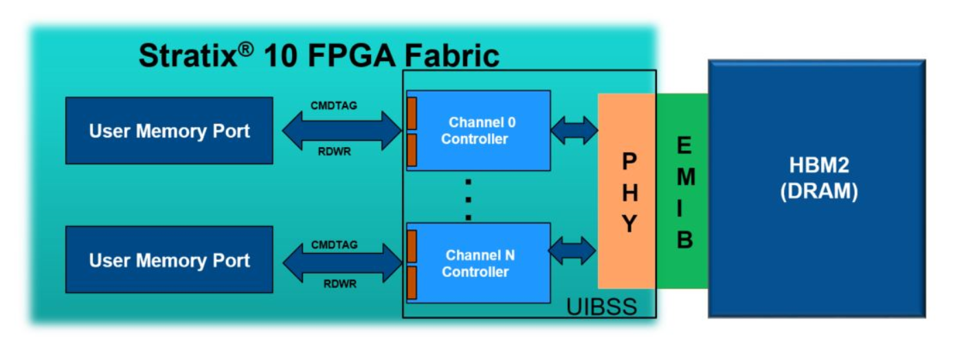
Intel® Stratix® 10 devices incorporate Intel’s Embedded Multi-Die Interconnect Bridge (EMIB) technology to implement a silicon bridge between HBM2 DRAM memory and the Universal Interface Block Subsystem (UIBSS), which contains the HBM2 controller (HBMC), physical-layer interface (PHY), and I/O ports to interface to the HBM2 stack.
As illustrated below, each Intel® Stratix® 10 device contains a single universal interface bus per HBM2 interface, supporting 8 independent channels.
The user interface to the HBM2 controller is maintained through the AXI4 protocol. Sixteen AXI interfaces are available in the user interface from each HBM2 controller, with one AXI interface available per HBM2 Pseudo Channel. HBM2 DRAM density of 4GB and 8GB are supported.
