High Bandwidth Memory (HBM2) Interface Intel® FPGA IP User Guide
ID
683189
Date
1/20/2023
Public
A newer version of this document is available. Customers should click here to go to the newest version.
1. About the High Bandwidth Memory (HBM2) Interface Intel® FPGA IP
2. Introduction to High Bandwidth Memory
3. Intel® Stratix® 10 HBM2 Architecture
4. Creating and Parameterizing the High Bandwidth Memory (HBM2) Interface Intel® FPGA IP
5. Simulating the High Bandwidth Memory (HBM2) Interface Intel® FPGA IP
6. High Bandwidth Memory (HBM2) Interface Intel® FPGA IP Interface
7. High Bandwidth Memory (HBM2) Interface Intel® FPGA IP Controller Performance
8. High Bandwidth Memory (HBM2) Interface Intel® FPGA IP User Guide Archives
9. Document Revision History for High Bandwidth Memory (HBM2) Interface Intel® FPGA IP User Guide
4.2.1. General Parameters for High Bandwidth Memory (HBM2) Interface Intel® FPGA IP
4.2.2. FPGA I/O Parameters for High Bandwidth Memory (HBM2) Interface Intel® FPGA IP
4.2.3. Controller Parameters for High Bandwidth Memory (HBM2) Interface Intel® FPGA IP
4.2.4. Diagnostic Parameters for High Bandwidth Memory (HBM2) Interface Intel® FPGA IP
4.2.5. Example Designs Parameters for High Bandwidth Memory (HBM2) Interface Intel® FPGA IP
4.2.6. Register Map IP-XACT Support for HBM2 IP
5.1. High Bandwidth Memory (HBM2) Interface Intel® FPGA IP Example Design
5.2. Simulating High Bandwidth Memory (HBM2) Interface Intel® FPGA IP with ModelSim* and Questa*
5.3. Simulating High Bandwidth Memory (HBM2) Interface Intel® FPGA IP with Synopsys VCS*
5.4. Simulating High Bandwidth Memory (HBM2) Interface Intel® FPGA IP with Riviera-PRO*
5.5. Simulating High Bandwidth Memory (HBM2) Interface Intel® FPGA IP with Cadence Xcelium* Parallel Simulator
5.6. Simulating High Bandwidth Memory (HBM2) Interface Intel® FPGA IP for High Efficiency
5.7. Simulating High Bandwidth Memory (HBM2) Interface IP Instantiated in Your Project
6.1. High Bandwidth Memory (HBM2) Interface Intel® FPGA IP High Level Block Diagram
6.2. High Bandwidth Memory (HBM2) Interface Intel® FPGA IP Controller Interface Signals
6.3. User AXI Interface Timing
6.4. User APB Interface Timing
6.5. User-controlled Accesses to the HBM2 Controller
6.6. Soft AXI Switch
7.1. High Bandwidth Memory (HBM2) DRAM Bandwidth
7.2. High Bandwidth Memory (HBM2) Interface Intel® FPGA IP HBM2 IP Efficiency
7.3. High Bandwidth Memory (HBM2) Interface Intel® FPGA IP Latency
7.4. High Bandwidth Memory (HBM2) Interface Intel® FPGA IP Timing
7.5. High Bandwidth Memory (HBM2) Interface Intel® FPGA IP DRAM Temperature Readout
6.4.2. APB Interface Timing
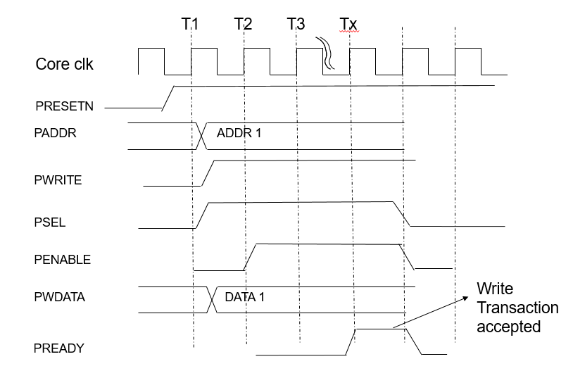
Write Access
Referring to the following diagram, write transactions to the APB interface follow these steps:
- At T1, a write transfer starts with address ADDR1, write data DATA1, write signal PWRITE and select signal PSEL registered at the rising edge of the core clock. This is the setup phase of the write transfer.
- At T2, PENABLE is registered at the rising edge of the core clock and held HIGH until the HBM2 controller asserts PREADY HIGH. The values of PADDR, PSEL, PENABLE, PWDATA, PSTRB and PWRITE must remain unchanged while PREADY remains LOW.
- At Tx, when PREADY goes HIGH, the write transaction completes at the next rising edge of the core clock. This indicates the end of the Write Access Phase. PREADY stays HIGH only for one clock cycle.
- PENABLE is deasserted at the end of the transfer. The select signal PSEL, is also deasserted unless the transfer is to be followed immediately by another transfer.
Figure 28. APB Write Transaction
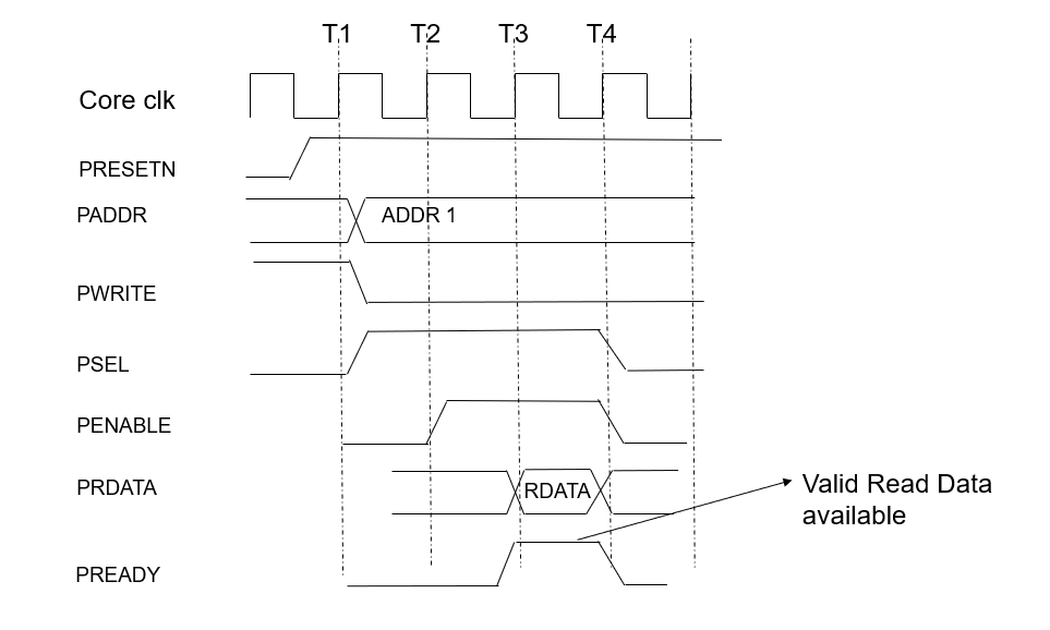
Read Access
Referring to the following diagram, read transactions to the APB interface follow these steps:
- At T1, a read transfer starts with address ADDR1, PWRITE asserted LOW and select signal PSEL registered at the rising edge of the core clock. This is the setup phase of the write transfer.
- At T2, PENABLE is registered at the rising edge of the core clock and held HIGH until the HBM2 controller asserts PREADY HIGH. The values of PADDR, PSEL, PENABLE and PWRITE must remain unchanged while PREADY remains LOW.
- At Tx, when PREADY goes HIGH, Read Data is available on the PRDATA bus. PREADY stays HIGH only for one clock cycle.
- PENABLE is deasserted at the end of the transfer. The select signal PSEL, is also deasserted unless the transfer is to be followed immediately by another transfer.
Figure 29. APB Read Transaction