6.2.6. AXI User-interface Signals
AXI Interface Signals
Each AXI port consists of five subchannels:
- Write Address Channel –AXI Write Address that maps to the HBM2 DRAM Write Address.
- Write Data Channel – AXI Write data provided by the core logic corresponding to the Write Address.
- Write Response Channel – Response from the HBM2 controller on the status of the Writes.
- Read Address Channel – AXI Read Address that maps to the HBM2 DRAM Read Address.
- Read Data Channel – AXI Read Data provided from the corresponding HBM2 DRAM Read Address.
AXI ID Definition
- The AXI burst transactions greater than 2 are available beginning in the Intel® Quartus® Prime software version 20.3. When the burst transactions are enabled through the HBM2 IP GUI, the width of arid/awid is set to [9 – ceil(log2(maximum burst length))], where up to 256 can be set as the maximum burst length.
- Burst transactions greater than 2 cannot be used with the soft AXI switch.
- When the soft AXI switch is not enabled, the AXI ID is 9-bits wide. A total of 29 AXI IDs are supported.
- When the soft AXI switch is enabled, the AXI ID is 7-bits wide. A total of 27 AXI IDs are supported.
AXI Address Definition
The HBM2 DRAM addressing consists of the following:
- 14-bit wide Row Address.
- 6-bit wide Column Address. The user logic drives Column Address bits COL[5:1], while the controller sets the lower order Column Address bit COL[0] to 0. For BL8 transactions, the user logic sets COL[1] to 0.
- 4-bit wide Bank Address. Bank Group corresponds to the higher order 2 bits of the Bank Address (BA[3:2]).
- 1-bit wide Stack ID(SID) available only in the 8GB configuration.
- 2-bit wide Slave ID, available only when the soft 4x×4 AXI switch is enabled through the HBM2 IP parameter editor.
The AXI Address Definition figure illustrates the mapping of the AXI Address bus (28-bit wide for 4GB configurations and 29-bit wide for 8GB configurations) for the various address ordering schemes to address the HBM2 DRAM, when the soft AXI switch is not used. The Address Definition with AXI Switch Enabled figure shows the AXI address definition when you have enabled the soft AXI switch. Refer to the AXI Interface Signals and Soft AXI Switch sections, for information for when the soft AXI switch is enabled.
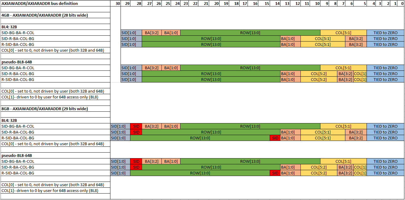
The Slave ID - SID[1:0] refers to the PC being accessed. The slave ID is available only when you have enabled the soft switch. For example, for a switch enabled in CH0 and CH1:
SID:00 - Ch0 PC0; SID: 01 - CH0 PC1;
SID:10 - CH1 PC0; SID:11 - CH1 PCH 1
AXI Burst Transactions
AXI burst transactions greater than 2 are available beginning in the Intel® Quartus® Prime software version 20.3. Burst transactions greater than burst length 2 are supported on the AWLEN/ARLEN inputs of the AXI interface in the BL4 Mode (that is, when the pseudo-BL8 mode is disabled through the HBM2 IP GUI). This feature is available when the AXI Switch is disabled and you have not selected the AVMM Interface mode. Support for this feature is added in the soft logic adapter for the Hard HBM Controller (HBMC).
This feature has the following specifications and requirements:
- Enabling AXI burst transactions through the HBM2 IP GUI:
- To enable the feature, select Enable the AXI Burst length of more than 2 in the Controller Tab of the parameter editor.
- Provide the AXI Maximum burst length value – a maximum value of 256 is allowed. Any AXI transaction can have an AWLEN/ARLEN value of 0 to the value configured in the AXI Maximum burst length minus 1, where the maximum burst length is set in the parameter editor. For example, if you enter a maximum burst length value of 3, the valid AWLEN/ARLEN values are from 0 to 2.
Figure 21. Parameters to Enable BL>2 and Set Maximum Burst Length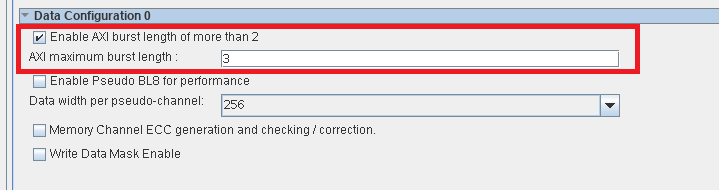
- The sequential address ordering required for the burst transactions is managed by the soft logic adaptor. You provide the starting AXI address of the transaction and the length of transaction (AWLEN/ARLEN).
- AWREADY/ARREADY is asserted once (along with AWVALID/ARVALID) to capture the start address and the current burst size. When AXI burst transactions are enabled, the HBM2 IP does not accept any new commands until the previous burst transaction is served. Consequently, AWREADY/ARREADY is de-asserted after the start address and the burst size are captured, until all addresses within the burst are issued internally.
- Transaction ID (AWID/ARID) widths are reduced to accommodate having internal IDs with the sliced bursts. When using this feature, the ID width is reduced to [9 bits – ceil(log2(maximum burst length))].
- You should take care to provide the correct address range, so that you do not accidentally write into unintended address space.
- You should also ensure the burst does not exceed 4KB of data as specified by the AXI4 spec. (Each AXI transaction in BL4 configuration provides 32B of data).
- You must handle buffering of data if the Controller READY is not asserted HIGH.
- WLAST signal should be asserted HIGH on the last burst data.
- Response ID width follows the ARID/AWID width.
- The read response follows the write transactions and has the RLAST pulse HIGH at the last transaction.
- Write response is provided for each Write command.
- ARSIZE/AWSIZE are not used and are not monitored by the controller.
The following HBM2 IP features are not available when using burst length values greater than 2:
- High efficiency pattern and mixed traffic in the Example design traffic generator.
- Efficiency monitor (under Diagnostics -> Enable efficiency monitor)
- AXI 4x4 soft switch.
- AVMM interface.
AXI Subchannels Descriptions
The syntax for referencing AXI port signal names is axi_x_y_portname where x is the channel number and y is the Pseudo Channel number. For example, axi_0_1_awid refers to the write address ID of the AXI port corresponding to channel 0 and Pseudo Channel 1. This applies to the bottom HBM2 interface.
For each channel in the top HBM2 interface, the AXI port for Pseudo Channel 0 is actually connected to the HBM2 memory for Pseudo Channel 1, and vice versa. This does not affect the HBM2 memory operation, but note that the Advanced Peripheral Bus (APB) register addresses for Pseudo Channel 0 are referring to Pseudo Channel 1, and vice versa.
The signals in the following tables refer to the signal names corresponding to a single AXI port: Channel 0, Pseudo Channel 0.
| Port Name | Width | Direction | Description | ||||||||||||
|---|---|---|---|---|---|---|---|---|---|---|---|---|---|---|---|
| axi_0_0_awid | 7 (AXI switch enabled) 9 (AXI switch not enabled) [9 – ceil(log2(maximum burst length))] (AXI Burst transactions enabled through HBM2 IP GUI) |
Input | Write address ID. This signal is the ID tag for the write address group of signals. This signal is 7-bits wide when the soft 4×4 AXI switch is enabled and 9-bits wide when the soft AXI switch is not enabled. When you enable the soft AXI Switch, this signal is 7-bits wide. When the soft 4×4 AXI switch is not enabled, the signal width is affected by the AXI burst transaction feature and the maximum burst length set through the HBM2 IP GU. When you enable AXI burst transactions, the width is reduced to [9 bits – ceil(log2(maximum burst length))]. When the AXI Burst transactions are not enabled, the width is 9 bits. |
||||||||||||
| axi_0_0_awaddr | 28/29 (AXI switch not enabled) 30/31 (AXI switch enabled) |
Input | Write address. The write address gives the address of the first transfer in a write burst transaction. This address bus is 28 bits wide for a 4 GB device and 29 bits for an 8 GB HBM2 device. When you enable the soft AXI switch, the higher-order 2-bits provide the slave address. |
||||||||||||
| axi_0_0_awlen | 8 | Input | Burst Length. The burst length gives the exact number of transfers in a burst. This information determines the number of data transfers associated with the address. Beginning in the Intel® Quartus® Prime software version 20.3, for the Burst Length 4 mode, more than 2 burst transactions up to a maximum value of 256 at the AXI Interface is supported. To use this feature, you must select Enable AXI Burst length of more than 2 and select a maximum burst length value in the HBM2 IP parameter editor. If this feature is not selected, then the following values are supported.
|
||||||||||||
| axi_0_0_awsize | 3 | Input | Burst Size. This signal indicates the size of each transfer in the burst.
The HBM2 controller supports only 256 bits, or 32 Bytes, of data transfers at the AXI Interface per AXI clock cycle. The HBM2 controller sets the value of axi_awsize and ignores any non-supported value driven through the axi_awsize port. |
||||||||||||
| axi_0_0_awburst | 2 | Input | The burst type and the size information, determined how the address for each transfer within the burst is calculated.
Only INCR is supported. The HBM2 controller sets the value of axi_awburst and ignores any non-supported value driven through the axi_awburst port. |
||||||||||||
| axi_0_0_awprot | 3 | Input | Protection Type. [Reserved for Future Use] This signal indicates the privilege and security level of the transaction, and whether the transaction is a data access or an instruction access.
|
||||||||||||
| axi_0_0_awqos | 4 | Input | Quality of Service. The Quality of Service identifier sent for each write transaction.
|
||||||||||||
| axi_0_0_awuser | 1 | Input | User Signal for auto-precharge.
Optional user-defined auto-precharge signal in the write address channel. |
||||||||||||
| axi_0_0_awvalid | 1 | Input | Write Address Valid. Indicates that the channel is signaling valid write address and control information. | ||||||||||||
| axi_0_0_awready | 1 | Output | Write Address Ready. Indicates that the slave is ready to accept an address and associated control signals. |
| Port Name | Width | Direction | Description |
|---|---|---|---|
| axi_0_0_wdata | 256 | Input | Write Data. |
| axi_0_0_wstrb | 32 | Input | Write Strobes (Byte Enables). Indicates which byte lanes (for axi_0_0_wdata) hold valid data. There is one write strobe bit for every eight bits of write data. |
| axi_extra_0_0_wuser_data | 32 | Input | Extra Write Data (AXI WUSER port). Carries additional write data when AXI Data Width of 288-bits data is selected in the HBM2 IP GUI. When 256 bits data is chosen in the GUI, this bus should be left undriven. |
| axi_extra_0_0_wuser_strb | 4 | Input | Extra Write Strobes (AXI WUSER port). Indicates which byte lanes (for axi_extra_0_0_wuser_data) hold valid data. This bus is used only when the AXI Data width of 288 bits is chosen in the HBM2 IP GUI. These signals should be left undriven when the data width is selected as 256 bits. |
| axi_0_0_wlast | 1 | Input | Write Last. Indicates the last transfer in a write burst. |
| axi_0_0_wvalid | 1 | Input | Write Valid. Indicates that valid write data and strobes are valid. |
| axi_0_0_wready | 1 | Output | Write Ready. Indicates that the slave (HBM2 controller) can accept write data.
Note: You should not provide write data during calibration in response to wready signal; refer to AXI Subchannels Descriptions for more details.
|
| Port Name | Width | Direction | Description |
|---|---|---|---|
| axi_0_0_bid | 7 (AXI switch enabled) 9 (AXI switch not enabled) |
Output | Response ID Tag. The ID tag of the write response. |
| axi_0_0_bresp | 2 | Output | Write response. Indicates the status of the write transaction.
|
| axi_0_0_bvalid | 1 | Output | Write response valid. Indicates that the channel is signaling a valid write response. |
| axi_0_0_bready | 1 | Input | Response ready. Indicates that the master can accept a write response. |
| Port Name | Width | Direction | Description | ||||||||||||
|---|---|---|---|---|---|---|---|---|---|---|---|---|---|---|---|
| axi_0_0_arid | 7 (AXI switch enabled) 9 (AXI switch not enabled) [9 – ceil(log2(maximum burst length))] (AXI Burst transactions enabled through HBM2 IP GUI). |
Input | Read address ID. The ID tag for the read address group of signals. This signal is 7-bits wide when the soft 4x4 AXI Switch is enabled and 9-bits wide when the soft AXI Switch is not enabled.s. When you enable the soft AXI Switch, this signal is 7-bits wide. When the soft 4×4 AXI switch is not enabled, the signal width is affected by the AXI burst transaction feature and the maximum burst length set through the HBM2 IP parameter editor. When the AXI burst transactions are enabled, the width is reduced to [9 bits – ceil(log2(maximum burst length))]. When AXI Burst transactions are not enabled, the width is 9 bits. |
||||||||||||
| axi_0_0_araddr | 28/29 (AXI switch not enabled) 30/31 (AXI switch enabled) |
Input | Read address. The address of the first transfer in a read burst transaction. This address bus is 28-bits wide for a 4 GB device and 29-bits wide for an 8 GB device. When you enable the soft AXI switch, the higher order 2-bits provide the slave address. |
||||||||||||
| axi_0_0_arlen | 8 | Input | Burst Length. The burst length gives the exact number of transfers in a burst. This information determines the number of data transfers associated with the address. Beginning in the Intel® Quartus® Prime software version 20.3, for the Burst Length 4 mode, more than 2 burst transactions up to a maximum value of 256 at the AXI Interface is supported. To use this feature, you must select Enable AXI Burst length of more than 2 and select a maximum burst length value in the HBM2 IP parameter editor. If this feature is not selected, then the following values are supported.
|
||||||||||||
| axi_0_0_arsize | 3 | Input | Burst Size. This signal indicates the size of each transfer in the burst.
The HBM2 controller supports only 256-bits, or 32 Bytes, of data transfers at the AXI Interface per AXI clock cycle. The HBM2 controller sets the value of axi_arsize and ignores any non-supported value driven through the axi_arsize port. |
||||||||||||
| axi_0_0_arburst | 2 | Input | The burst type and the size information, determined how the address for each transfer within the burst is calculated.
Only INCR is supported. The HBM2 controller sets the value of axi_arburst and ignores any non-supported value driven through the axi_0_0_arburst port. |
||||||||||||
| axi_0_0_arprot | 3 | Input | Protection Type. [Reserved for Future Use] Indicates the privilege and security level of the transaction, and whether the transaction is a data access or an instruction access.
|
||||||||||||
| axi_0_0_arqos | 4 | Input | Quality of Service. The Quality of Service identifier sent for each write transaction.
|
||||||||||||
| axi_0_0_aruser | 1 | User Signal for auto-precharge.
|
|||||||||||||
| axi_0_0_arvalid | 1 | Input | Read address valid. Indicates that the channel signals valid read address and control information. | ||||||||||||
| axi_0_0_arready | 1 | Output | Read address ready. Indicates that the slave is ready to accept an address and associated control signals. |
| Port Name | Width | Direction | Description |
|---|---|---|---|
| axi_0_0_rid | ARID_WIDTH | Output | Read ID tag. The ID tag for the read data group of signals generated by the slave. |
| axi_0_0_rdata | 256 | Output | Read data. |
| axi_extra_0_0_ruser_data | 32 | Output | Extra Read Data (AXI RUSER port). Carries the extra read data when the data width of 288 is chosen in the HBM2 IP GUI. This bus can be left unconnected when a 256 Data option is chosen in the HBM2 IP GUI. |
| axi_extra_0_0_ruser_err_dbe | 1 | Output | Double-Bit-Error (AXI RUSER port). Carries DBE information. 1’b1 indicates error. |
| axi_0_0_rresp | 2 | Output | Read response. Indicates the status of the read transfer:
|
| axi_0_0_rlast | 1 | Output | Read last. Indicates the last transfer in a read burst. |
| axi_0_0_rvalid | 1 | Output | Read valid. Indicates that the channel is signaling the required read data. All AXI Read data Channel output signals that output from the HBM2 Controller are provided aligned to the axi_0_0_rvalid signal. |
| axi_0_0_rready | 1 | Input | Read ready. Indicates that the master can accept the read data and response information. |