4.2.1. General Parameters for High Bandwidth Memory (HBM2) Interface Intel® FPGA IP
| Display Name | Description |
|---|---|
| Speed Grade | Speed grade of FPGA device and whether it is an engineering sample (ES) or a production device. The value is automatically determined based on the device selected under . If you do not specify a device, the system assumes a production device of the fastest speed grade. You should always specify the correct target device during IP generation; failure to specify the correct device may result in generated IP that does not work on hardware. Specifies the speed grade of the Intel® Stratix® 10 FPGA. |
| HBM2 Location | Determines the location of the HBM2 interface in the Intel® Stratix® 10 FPGA. The FPGA offers HBM2 interfaces on the top and bottom of the FPGA core. |
| HBM2 Device Type | The HBM device type. 4GB/4H refers to HBM2 device with a total device density of 4GB in a 4-high Stack, and 8GB8H refers to a total HBM2 device density of 8GB in an 8-high Stack. |
| Display Name | Description |
|---|---|
| Channel 0 and 1 Interface Settings (Applies to HBM2 Channels 2 and 3, 4 and 5, 6 and 7) | |
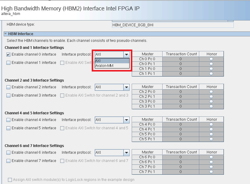
| Enable Channel 0 interface | Adds a High Bandwidth Memory controller on channel 0 of the Universal Interface Block. Each controller handles two HBM Pseudo Channels. You can select the HBM2 memory channels that you want to implement. Each HBM2 channel supports a 128-bit interface to the HBM2 device, using two 64-bit Pseudo Channels. The user interface to the HBM2 controller uses the AXI4 protocol. Each controller has one AXI4 interface per Pseudo Channel or two AXI4 interfaces per channel. |
| Enable Channel 1 interface | Adds a High Bandwidth Memory controller on channel 1 of the Universal Interface Block. Each controller handles two HBM Pseudo Channels. You can select the HBM2 memory channels that you want to implement. Each HBM2 channel supports a 128-bit interface to the HBM2 device, using two 64-bit Pseudo Channels. The user interface to the HBM2 controller uses the AXI4 protocol. Each controller has one AXI4 interface per Pseudo Channel or two AXI4 interfaces per channel. |
| Interface Protocol | The Interface protocol can be selected per channel pair (0 and 1, 2 and 3, 4 and 5, 6 and 7). The following protocols are supported:
|
| Enable AXI Switch for channel 0 and 1 | Adds soft AXI switch logic that enables each AXI master to access the entire memory space of Channels 0 and 1 in HBM2 DRAM. The soft AXI switch is available only when you select the AXI Interface Protocol. Refer to Soft AXI Switch for information on using the AXI switch.
Note: You must enable two HBM2 channels to access the corresponding 4x4 AXI switch.
|
| Master | Enables selection of arbitration schemes to provide efficient memory access for each AXI master. |
| Transaction Count | Provide the total transaction count that the master intends to issue when provided access. Each transaction count refers to a single BL4 or pseudo-BL8 transaction. The total transaction count includes transaction counts to all the Pseudo Channels that the master intends to issue when provided access. The default value is 0. The HBM2 IP can support a maximum of 65535 transactions. Be aware that high transaction counts can reduce fabric performance. Refer to AXI Switch Selection in HBM2 IP Catalog for information on transaction count. |
| Honor | Select the master that requires higher priority over other masters. You can choose only one master; if you do not choose a master, all masters receive the same priority and round robin arbitration is followed. |
| Display Name | Description |
|---|---|
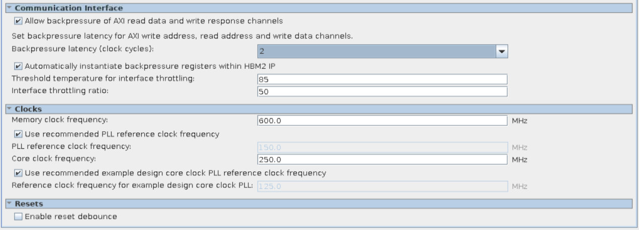
| Allow backpressure of AXI read data and write response channels | Instantiates FIFOs in soft logic to buffer read data and write response on the AXI interfaces. This is required if the RREADY/BREADY signals are ever deasserted. You can disable this option to reduce latency but only if RREADY/BREADY are never used to backpressure the interface. The backpressure feature is available only in the AXI under-interface flow; it is not available in the Avalon® memory-mapped interface flow. |
| Backpressure latency (clock cycles) | Select a value from 0 to 2 (0 is the default). Allows the user interface time to react to the controller READY signals (AXI Write Address / Read Address / Write Data) and can also be used to improve timing between the AXI User Interface and the HBM2 IP with no increase in latency. |
| Automatically instantiate backpressure registers within the HBM2 IP | This option is available beginning in the Intel® Quartus® Prime software version 20.3. This option allows you to let the HBM2 IP place the back pressure registers within the IP or place the registers manually as needed. The design example places the backpressure registers inside the HBM2 IP. Refer to Improving User Logic to HBM2 Controller AXI Interface Timing for information on using this feature.
Note:
From Intel® Quartus® Prime software version 19.4 through 20.2, the backpressure registers were internally generated within the HBM2 IP; in releases earlier than 19.4, you were required to implement these registers as needed, manually. |
| Threshold temperature for AXI throttling | This parameter defines the temperature of the HBM2 stack, in degrees Celsius, above which the HBM2 controller throttles AXI interface transactions. The temperature setting applies to all the AXI4 interfaces; however, you must enable this feature on the corresponding controller tab of each HBM2 controller. When you enable throttling, the HBM2 controller reduces the amount of traffic on the DRAM channel. |
| AXI throttling ratio | If AXI interface throttling is enabled based on temperature this parameter defines the throttle ratio as a percentage (0 = no throttling, 100 = full throttling). You can enable or disable throttling on the individual controller tabs. |
| Display Name | Description |
|---|---|
| Enable reset debounce | If enabled, reset debouncing logic is added on the wmcrst_n_in signal |
| Debounce period | Set the debounce period in ms. The minimum period is 20 ms. |
| Display Name | Description |
|---|---|
| Memory clock frequency | The frequency of the memory clock in MHz. Specifies the clock frequency for the HBM2 interface. The maximum supported HBM2 clock frequency depends on the FPGA device speed grade:
|
| Use recommended PLL reference clock frequency | When checked the PLL reference clock frequency is automatically calculated for best performance. Uncheck the check box if you want to specify your own PLL reference clock frequency. Automatically calculates the PLL reference clock frequency for best performance. You should disable this parameter if you want to select a different PLL reference clock frequency |
| PLL reference clock frequency | PLL reference clock frequency. This is a universal interface bus (UIB) PLL reference clock. You must feed a clock of this frequency to the PLL reference clock input of the memory interface. Enable this parameter only if you disable Use recommended PLL reference clock frequency, and want to specify a PLL reference clock frequency. You should use the fastest possible PLL reference clock frequency to achieve best jitter performance. |
| Core clock frequency | The frequency of the user AXI4 interface in MHz. This clock must be provided from an I/O PLL (not instantiated by the HBM2 IP). The reference clock driving the core I/O PLL must be provided from the same oscillator that supplies the UIB PLL reference clock on the board for a given HBM2 interface, to achieve maximum performance. The maximum supported core frequency depends on the device speed grade and timing closure of the core interface clock within the FPGA. The minimum frequency of the core clock is one-fourth the HBM2 interface frequency. Intel® does not guarantee timing closure of the HBM2 IP core logic above the recommended core clock frequencies shown in Table 9, when the maximum supported HBM2 interface frequency is selected. You may still run your design above the recommended values and within the maximum allowable range, but core timing closure may be difficult— Intel® does not provide support for such timing closure failure. Techniques such as using logic lock regions and/or design partitions may help with timing closure. |
| Use recommended example design core clock PLL reference clock frequency | Automatically calculates the PLL reference clock frequency for best performance. Uncheck the check box if you want to specify your own PLL reference clock frequency. Automatically calculates the example design core clock PLL reference clock frequency for best performance. Disable this parameter if you want to select a different reference clock frequency. |
| Reference clock frequency for example design core clock PLL | The PLL reference clock frequency in MHz for the PLL supplying the core clock. This parameter is used only in the example design PLL. Specify the externally provided reference clock frequency for the core clock PLL. |
| Speed Grade | Maximum HBM2 Interface Frequency | Minimum Allowable Core Clock (Hardware Limit) | Maximum Allowable Core Clock (Hardware Limit) | Recommended Maximum Core Clock Frequency |
|---|---|---|---|---|
| -3 | 600 MHz | 150 MHz | 300 MHz | 300 MHz |
| -2 | 800 MHz | 200 MHz | 400 MHz | 370 MHz |
| -1 | 1 GHz | 250 MHz | 500 MHz | 405 MHz |