High Bandwidth Memory (HBM2) Interface Intel® FPGA IP User Guide
ID
683189
Date
1/20/2023
Public
A newer version of this document is available. Customers should click here to go to the newest version.
1. About the High Bandwidth Memory (HBM2) Interface Intel® FPGA IP
2. Introduction to High Bandwidth Memory
3. Intel® Stratix® 10 HBM2 Architecture
4. Creating and Parameterizing the High Bandwidth Memory (HBM2) Interface Intel® FPGA IP
5. Simulating the High Bandwidth Memory (HBM2) Interface Intel® FPGA IP
6. High Bandwidth Memory (HBM2) Interface Intel® FPGA IP Interface
7. High Bandwidth Memory (HBM2) Interface Intel® FPGA IP Controller Performance
8. High Bandwidth Memory (HBM2) Interface Intel® FPGA IP User Guide Archives
9. Document Revision History for High Bandwidth Memory (HBM2) Interface Intel® FPGA IP User Guide
4.2.1. General Parameters for High Bandwidth Memory (HBM2) Interface Intel® FPGA IP
4.2.2. FPGA I/O Parameters for High Bandwidth Memory (HBM2) Interface Intel® FPGA IP
4.2.3. Controller Parameters for High Bandwidth Memory (HBM2) Interface Intel® FPGA IP
4.2.4. Diagnostic Parameters for High Bandwidth Memory (HBM2) Interface Intel® FPGA IP
4.2.5. Example Designs Parameters for High Bandwidth Memory (HBM2) Interface Intel® FPGA IP
4.2.6. Register Map IP-XACT Support for HBM2 IP
5.1. High Bandwidth Memory (HBM2) Interface Intel® FPGA IP Example Design
5.2. Simulating High Bandwidth Memory (HBM2) Interface Intel® FPGA IP with ModelSim* and Questa*
5.3. Simulating High Bandwidth Memory (HBM2) Interface Intel® FPGA IP with Synopsys VCS*
5.4. Simulating High Bandwidth Memory (HBM2) Interface Intel® FPGA IP with Riviera-PRO*
5.5. Simulating High Bandwidth Memory (HBM2) Interface Intel® FPGA IP with Cadence Xcelium* Parallel Simulator
5.6. Simulating High Bandwidth Memory (HBM2) Interface Intel® FPGA IP for High Efficiency
5.7. Simulating High Bandwidth Memory (HBM2) Interface IP Instantiated in Your Project
6.1. High Bandwidth Memory (HBM2) Interface Intel® FPGA IP High Level Block Diagram
6.2. High Bandwidth Memory (HBM2) Interface Intel® FPGA IP Controller Interface Signals
6.3. User AXI Interface Timing
6.4. User APB Interface Timing
6.5. User-controlled Accesses to the HBM2 Controller
6.6. Soft AXI Switch
7.1. High Bandwidth Memory (HBM2) DRAM Bandwidth
7.2. High Bandwidth Memory (HBM2) Interface Intel® FPGA IP HBM2 IP Efficiency
7.3. High Bandwidth Memory (HBM2) Interface Intel® FPGA IP Latency
7.4. High Bandwidth Memory (HBM2) Interface Intel® FPGA IP Timing
7.5. High Bandwidth Memory (HBM2) Interface Intel® FPGA IP DRAM Temperature Readout
4.2.2. FPGA I/O Parameters for High Bandwidth Memory (HBM2) Interface Intel® FPGA IP
Figure 8. FPGA I/O Tab
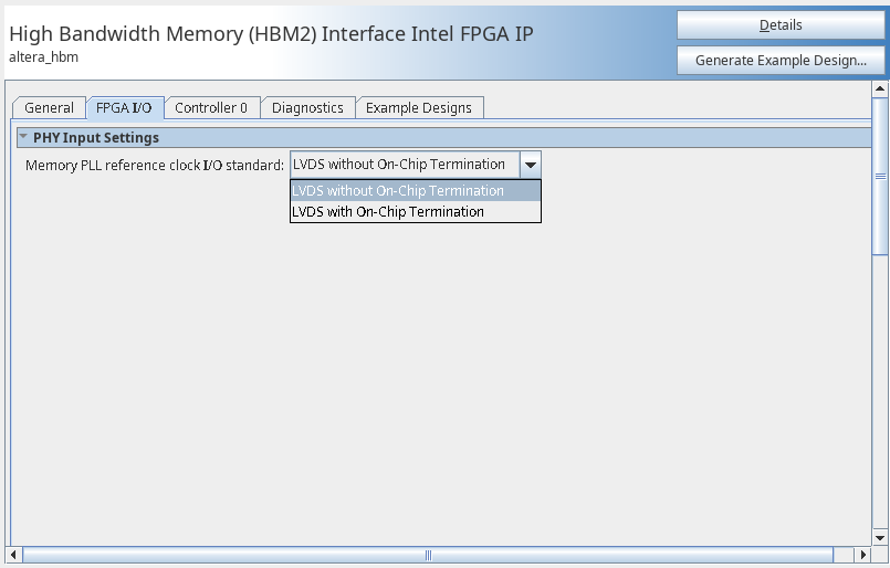
| Display Name | Description |
|---|---|
| Memory PLL Reference clock I/O standard | Specifies the I/O standard for the PLL reference clock of the memory interface. The termination options available are LVDS with on-chip termination and LVDS without on-chip termination. This parameter is available beginning with Intel® Quartus® Prime software version 20.3. For designs migrating from previous releases, LVDS without on-chip termination is selected. |