High Bandwidth Memory (HBM2) Interface Intel® FPGA IP User Guide
ID
683189
Date
1/20/2023
Public
A newer version of this document is available. Customers should click here to go to the newest version.
1. About the High Bandwidth Memory (HBM2) Interface Intel® FPGA IP
2. Introduction to High Bandwidth Memory
3. Intel® Stratix® 10 HBM2 Architecture
4. Creating and Parameterizing the High Bandwidth Memory (HBM2) Interface Intel® FPGA IP
5. Simulating the High Bandwidth Memory (HBM2) Interface Intel® FPGA IP
6. High Bandwidth Memory (HBM2) Interface Intel® FPGA IP Interface
7. High Bandwidth Memory (HBM2) Interface Intel® FPGA IP Controller Performance
8. High Bandwidth Memory (HBM2) Interface Intel® FPGA IP User Guide Archives
9. Document Revision History for High Bandwidth Memory (HBM2) Interface Intel® FPGA IP User Guide
4.2.1. General Parameters for High Bandwidth Memory (HBM2) Interface Intel® FPGA IP
4.2.2. FPGA I/O Parameters for High Bandwidth Memory (HBM2) Interface Intel® FPGA IP
4.2.3. Controller Parameters for High Bandwidth Memory (HBM2) Interface Intel® FPGA IP
4.2.4. Diagnostic Parameters for High Bandwidth Memory (HBM2) Interface Intel® FPGA IP
4.2.5. Example Designs Parameters for High Bandwidth Memory (HBM2) Interface Intel® FPGA IP
4.2.6. Register Map IP-XACT Support for HBM2 IP
5.1. High Bandwidth Memory (HBM2) Interface Intel® FPGA IP Example Design
5.2. Simulating High Bandwidth Memory (HBM2) Interface Intel® FPGA IP with ModelSim* and Questa*
5.3. Simulating High Bandwidth Memory (HBM2) Interface Intel® FPGA IP with Synopsys VCS*
5.4. Simulating High Bandwidth Memory (HBM2) Interface Intel® FPGA IP with Riviera-PRO*
5.5. Simulating High Bandwidth Memory (HBM2) Interface Intel® FPGA IP with Cadence Xcelium* Parallel Simulator
5.6. Simulating High Bandwidth Memory (HBM2) Interface Intel® FPGA IP for High Efficiency
5.7. Simulating High Bandwidth Memory (HBM2) Interface IP Instantiated in Your Project
6.1. High Bandwidth Memory (HBM2) Interface Intel® FPGA IP High Level Block Diagram
6.2. High Bandwidth Memory (HBM2) Interface Intel® FPGA IP Controller Interface Signals
6.3. User AXI Interface Timing
6.4. User APB Interface Timing
6.5. User-controlled Accesses to the HBM2 Controller
6.6. Soft AXI Switch
7.1. High Bandwidth Memory (HBM2) DRAM Bandwidth
7.2. High Bandwidth Memory (HBM2) Interface Intel® FPGA IP HBM2 IP Efficiency
7.3. High Bandwidth Memory (HBM2) Interface Intel® FPGA IP Latency
7.4. High Bandwidth Memory (HBM2) Interface Intel® FPGA IP Timing
7.5. High Bandwidth Memory (HBM2) Interface Intel® FPGA IP DRAM Temperature Readout
3.3. Intel® Stratix® 10 HBM2 Controller Architecture
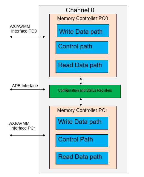
The hardened HBM2 controller provides a controller per Pseudo Channel.
Each controller consists of a write and read data path and the control logic that helps to translate user commands to the HBM2 memory. The HBM2 controller logic accounts for the HBM2 memory specification timing and schedules commands in an efficient manner. The following figure shows a block diagram of the HBM2 controller, corresponding to channel 0. The HBM2 controller's user-logic interface follows the AXI interface as well as the Avalon® memory-mapped interface (commencing in the Intel® Quartus® Prime software version 20.2. You can find more information about the interface timing details in the User AXI Interface Timing section.
Figure 5. Intel® Stratix® 10 HBM2 Controller Block Diagram