6.5.1. User-controlled Refreshes
If you want to allow user logic to issue Refresh requests, you must specify so in the Controller Settings of the parameter editor, as follows:
Change the value from Controller Refresh All to User Refresh All or User Refresh Per-bank.
Each APB interface corresponds to one HBM2 channel, therefore requests must be addressed to either of the two Pseudo Channels, one Pseudo Channel at a time.
The timing of the refresh interval is specific to the HBM2 DRAM timing. The required refresh rate is provided by the HBM2 DRAM through the TEMP[2:0] vector, which can be read through the APB interface.
| TEMP[2:0] | Refresh Rate |
|---|---|
| 000 | 4x tREFI |
| 001 | 2x tREFI |
| 011 | 1x tREFI |
| 010 | 0.5x tREFI |
| 110 | 0.25x tREFI |
| 111 | TBD |
| 101 | TBD |
| 100 | TBD |
Refresh command options available from user logic are as follows:
- User refresh commands issued on a per bank basis. This corresponds to banks corresponding to the HBM2 Pseudo Channel.
- User refresh commands to all banks. This corresponds to all banks corresponding to the HBM2 Pseudo Channel.
- Self-refresh command.
All the user refresh requests follow the APB interface protocol. User logic issues the Refresh request and waits for the acknowledgement signal from the HBM2 controller before issuing another Refresh request.
User Refresh Per Bank
User refresh requests per-bank consist of the following commands issued to the APB Interface
| Write Data Definition for Refresh Request | Description |
|---|---|
| [0] | Pseudo Channel Number. Set the following values to indicate the Pseudo channel number: 0 - Pseudo Channel 0 1 - Pseudo Channel 1 |
| [5:1] | Bank number for per-bank refresh. Bit[5] - Stack ID in 8GB configuration. Bit[4:1] – 4-bit Bank Address. |
| [6] | Select Per bank or all bank refresh. Set to 1’b0 for per bank refresh. |
| [7] | Reserved. Set to 1'b0. |
| [8] | User initiated refresh request. Set this bit to 1’b1 to initiate refresh command. |
| [12:10] | Number of bursts for per bank refresh bursting feature. Burst = value[1:0] + 1. The per-bank refresh bursting is a feature supported by the HBM2 controller where the user interface can request refresh commands to be issued to more than one HBM2 DRAM bank. |
| [15:13] | Increment value for per bank refresh bursting feature; rolls over once it reached the max bank value. Increment = value[2:0] + 1, where value refers to the current bank address when the write command is issued. This becomes the starting bank address.
Note: The ratio of maximum increment value to total number of banks per Pseudo Channel divided by 4. (For example, a 4H device has a maximum value of 16/4=4.)
|
To issue user refresh commands on a per-bank basis, follow these steps:
- Write to address 16’h0000 with corresponding Write Data.
- For example, Write data of 16’b0000_0001_0000_0010 (Pseudo-channel 0; bank address is located in Bits[5:1] ; Bit[6] set to 0 for per-bank refresh; Bit [8] set to User initiated Refresh Request).
- To issue multiple burst of per-bank refresh, set corresponding bits in PWDATA[12:10] and PWDATA[15:13] with desired settings.
- Read from address 16’h0000 for Refresh Request Acknowledge.
- Wait till PRDATA[9] returns 1’b1 to indicate refresh request is accepted by controller. You can ignore the values of all the other bits of PRDATA. The following figure explains the timing of per-bank refresh request to the APB Interface.
Figure 30. Timing of APB Refresh Request Per Bank
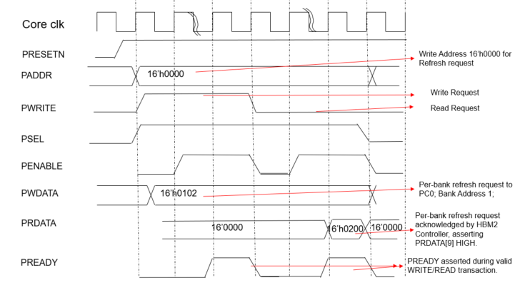
Individual requests to different Pseudo Channels must be issued serially. You must wait for the HBM2 controller to issue the Acknowledge signal before issuing another Refresh request.
User Refresh to All Banks
| Write Data Bit Definition for Refresh Request | Description |
|---|---|
| [0] | Pseudo Channel Number. Set a value of 0 for Pseudo Channel 0, or a value of 1 for Pseudo Channel 1. |
| [5:1] | Bank number for per-bank refresh. Ignored for All bank refresh. |
| [6] | Select Per bank or all bank refresh. Set to 1’b1 - all banks refresh. |
| [7] | Reserved. Set to 1'b0. |
| [8] | User initiated refresh request. Set this bit to 1’b1 to initiate refresh command. |
| [15:9] | Ignored. |
| Read Data Bit Definition for Refresh Request | Description |
|---|---|
| [8:0] | Reserved. |
| [9] | HBM2 controller-issued Refresh Request Acknowledge.
|
| [15:10] | Reserved. |
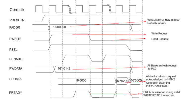
To issue user refresh commands to all banks, follow these steps:
- Write to address 16’h0000 with corresponding Write Data.
- For example, Write data of 16’b0000_0001_0100_0010 (Pseudo Channel 0; bank address is located in Bits[5:1] ; Bit[6] set to 1 for all-banks refresh; Bit [8] set to User initiated Refresh Request).
- Read to Address 16’h0000 for Refresh Request Acknowledge.
- Wait till PRDATA[9] returns a value of 1’b1 to indicate User Refresh request is accepted by the controller. The following figure explains the APB interface timing for refresh request to all banks.
Figure 31. Timing of APB Refresh Request to All Banks
Self Refresh
To enter a Self Refresh state, issue these commands to the APB interface:
- Write to address 16’h004 with Write Data(PWDATA) of 16’h0001.
- Read from address 16’h004. Wait until Read Data (PRDATA [1]) returns a value of 1’b1 to indicate that the HBM2 controller is in a Self Refresh state.
To exit a Self Refresh state, issue this command to the APB interface:
- Write to address 16’h0004 with Write Data(PWDATA) of 16’h0000 to exit Self-Refresh. Wait for the Self Refresh Acknowledge to be 1’b0 prior to issuing another Self Refresh request.
The write data bus is used to request entry or exit from self refresh. The Read data bus is used to read the self-refresh status of the HBM2 channel. The following tables provide the Write and Read data definitions for accessing self refresh.
| Write Data Bit Definition | Description |
|---|---|
| [0] | User-initiated Self-Refresh Request. To enter Self Refresh:
|
| [15:1] | Reserved. |
| Read Data Bit Definition | Description |
|---|---|
| [0] | Reserved. |
| [1] | Self refresh status:
|
| [15:2] | Reserved. |