Stratix V Avalon-ST Interface with SR-IOV PCIe Solutions: User Guide
ID
683488
Date
5/02/2016
Public
1. Datasheet
2. Getting Started with the SR-IOV DMA Example Design
3. Parameter Settings
4. Interfaces and Signal Descriptions
5. Registers
6. Programming and Testing SR-IOV Bridge MSI Interrupts
7. Error Handling
8. IP Core Architecture
9. Design Implementation
10. Transceiver PHY IP Reconfiguration
11. Debugging
A. Frequently Asked Questions for PCI Express
B. Transaction Layer Packet (TLP) Header Formats
C. Stratix V Avalon-ST with SR-IOV Interface for PCIe Solutions User Guide Archive
12. Document Revision History
1.1. Stratix® V Avalon-ST Interface with SR-IOV for PCIe Datasheet
1.2. Release Information
1.3. Device Family Support
1.4. Design Examples for SR-IOV
1.5. Debug Features
1.6. IP Core Verification
1.7. Performance and Resource Utilization
1.8. Recommended Speed Grades for SR-IOV Interface
1.9. Creating a Design for PCI Express
2.1. Generating the Example Design Testbench
2.2. Understanding the Generated Files and Directories
2.3. Simulating the SR-IOV Example Design
2.4. Running a Gate-Level Simulation
2.5. Understanding the DMA Functionality
2.6. Compiling the Example Design with the Quartus® Prime Software
2.7. Using the IP Catalog To Generate Your Stratix V Hard IP for PCI Express as a Separate Component
4.1. Avalon-ST TX Interface
4.2. Component-Specific Avalon-ST Interface Signals
4.3. Avalon-ST RX Interface
4.4. BAR Hit Signals
4.5. Configuration Status Interface
4.6. Clock Signals
4.7. Function-Level Reset Interface
4.8. Interrupt Interface
4.9. Configuration Extension Bus (CEB) Interface
4.10. Implementing MSI-X Interrupts
4.11. Local Management Interface (LMI) Signals
4.12. Reset, Status, and Link Training Signals
4.13. Transceiver Reconfiguration
4.14. Serial Data Signals
4.15. Test Signals
4.16. PIPE Interface Signals
5.1. Correspondence between Configuration Space Registers and the PCIe Specification
5.2. PCI and PCI Express Configuration Space Registers
5.3. MSI Registers
5.4. MSI-X Capability Structure
5.5. Power Management Capability Structure
5.6. PCI Express Capability Structure
5.7. Advanced Error Reporting (AER) Enhanced Capability Header Register
5.8. Uncorrectable Error Status Register
5.9. Uncorrectable Error Mask Register
5.10. Uncorrectable Error Severity Register
5.11. Correctable Error Status Register
5.12. Correctable Error Mask Register
5.13. Advanced Error Capabilities and Control Register
5.14. Header Log Registers 0-3
5.15. SR-IOV Virtualization Extended Capabilities Registers
5.16. Virtual Function Registers
5.15.1. SR-IOV Virtualization Extended Capabilities Registers Address Map
5.15.2. ARI Enhanced Capability Header
5.15.3. SR-IOV Enhanced Capability Registers
5.15.4. Initial VFs and Total VFs Registers
5.15.5. VF Device ID Register
5.15.6. Page Size Registers
5.15.7. VF Base Address Registers (BARs) 0-5
5.15.8. Secondary PCI Express Extended Capability Header
5.15.9. Lane Status Registers
11.1.1. Changing Between Serial and PIPE Simulation
11.1.2. Using the PIPE Interface for Gen1 and Gen2 Variants
11.1.3. Viewing the Important PIPE Interface Signals
11.1.4. Disabling the Scrambler for Gen1 and Gen2 Simulations
11.1.5. Disabling 8B/10B Encoding and Decoding for Gen1 and Gen2 Simulations
11.1.6. Changing between the Hard and Soft Reset Controller
2.1. Generating the Example Design Testbench
Follow these steps to generate the SR-IOV DMA example design testbench:
- Copy <install_dir>/ ip/altera/altera_pcie/altera_pcie_sriov/example_design/sriov_top_dma_gen3_x8_256b.qsys to your working directory. This top-level Qsys design includes three subsystems.
Qsys Subsystem Description sriov_dma_app_g3x8_256b.qsys This subsystem implements of the Read DMA read and Write DMA modules and the Read and Write Descriptor Controllers. the DMA engine. rddc_ctl_256b.qsys This subsystem implements the Read Descriptor Controller for 4 Read DMA channels. wrdc_ctl_256b.qsys This subsystem implements the Write Descriptor Controller for 4 Write DMA channels. - Rename the top-level Qsys file, sriov_top_dma_gen3_x8_256b.qsys, to top.qsys.
- In your working directory, start Qsys by typing the following command:
qsys-edit
- Open top.qsys.
The following figure shows the Qsys system.
Figure 3. Top-Level Qsys System for SR-IOV Gen3 x8 DMA Example Design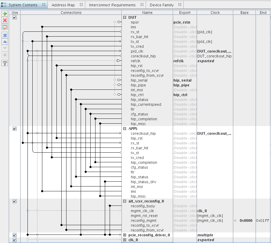
- On the Generate menu, select Generate Testbench System.
The Generation dialog box appears.
- Specify the following parameters:
Table 8. Parameters to Specify on the Generation Menu in Qsys Parameter
Value
Testbench System
Create testbench Qsys system
Standard, BFMs for standard Avalon interfaces.
Create testbench simulation model
Verilog. This option generates simulation files for the testbench.
Allow mixed-language simulation Leave this option off. Output Directory
Path
working_dir/ Testbench
working_dir/testbench/ - Click Generate.
Qsys generates the testbench.
- To generate files for compilation, on the Quartus® Prime Generate menu, select Generate HDL.
The Generation dialog box appears.
- Specify the following parameters:
Table 9. Parameters to Specify on the Generation Menu in Qsys Parameter
Value
Verilog
Create HDL design files for synthesis
Verilog.
Create timing and resource estimates for third-party EDA synthesis tools
Leave this option off.
Create block symbol file (.bsf) Leave this option on. Simulation
Create simulation model
None. (You created the simulation model when you generated the testbench.) Allow mixed language simulation
Leave this option off. Output Directory
Path
working_dir/top - Click Generate.
- On the File menu, click Save.