DSP Builder for Intel® FPGAs (Advanced Blockset): Handbook
ID
683337
Date
3/23/2022
Public
A newer version of this document is available. Customers should click here to go to the newest version.
1. About DSP Builder for Intel® FPGAs
2. DSP Builder for Intel FPGAs Advanced Blockset Getting Started
3. DSP Builder Design Flow
4. Primitive Library Blocks Tutorial
5. IP Tutorial
6. DSP Builder for Intel FPGAs (Advanced Blockset) Design Examples and Reference Designs
7. DSP Builder Design Rules, Design Recommendations, and Troubleshooting
8. About DSP Builder for Intel FPGAs Optimization
9. About Folding
10. Floating-Point Data Types
11. Design Configuration Library
12. IP Library
13. Interfaces Library
14. Primitives Library
15. Utilities Library
16. Simulink Supported Blocks
17. Document Revision History for DSP Builder for Intel FPGAs (Advanced Blockset) Handbook
2.1. Starting DSP Builder in MATLAB*
2.2. Browsing DSP Builder Libraries and Adding Blocks to a New Model
2.3. Browsing and Opening DSP Builder Design Examples
2.4. Creating a New DSP Builder Design with the DSP Builder New Model Wizard
2.5. Simulating, Verifying, Generating, and Compiling Your DSP Builder Design
3.1. Implementing your Design in DSP Builder Advanced Blockset
3.2. Verifying your DSP Builder Advanced Blockset Design in Simulink and MATLAB
3.3. Exploring DSP Builder Advanced Blockset Design Tradeoffs
3.4. Verifying your DSP Builder Design with C++ Software Models
3.5. Verifying your DSP Builder Advanced Blockset Design in the ModelSim Simulator
3.6. Verifying Your DSP Builder Design in Hardware
3.7. Integrating Your DSP Builder Advanced Blockset Design into Hardware
3.1.2.1. DSP Builder Block Interface Signals
3.1.2.2. Periods
3.1.2.3. Sample Rate
3.1.2.4. Building Multichannel Systems
3.1.2.5. Channelization for Two Channels with a Folding Factor of 3
3.1.2.6. Channelization for Four Channels with a Folding Factor of 3
3.1.2.7. Synchronization and Scheduling of Data with the Channel Signal
3.1.2.8. Simulink vs Hardware Design Representations
3.2.1. Verifying your DSP Builder Advanced Blockset Design with a Testbench
3.2.2. Running DSP Builder Advanced Blockset Automatic Testbenches
3.2.3. Using DSP Builder Advanced Blockset References
3.2.4. Setting Up Stimulus in DSP Builder Advanced Blockset
3.2.5. Analyzing your DSP Builder Advanced Blockset Design
3.6.2.3.1. Setting up Board Support Package for 28 nm Device Families
3.6.2.3.2. Setting up Board Support Packages for Other Device Families
3.6.2.3.3. Publishing the Package in the System-In-The-Loop Wizard
3.6.2.3.4. System-in-the-Loop Third-Party Board Support Packages
3.6.2.3.5. Template Values in the System-in-the-Loop boardinfos.xml File
4.1. Creating a Fibonacci Design from the DSP Builder Primitive Library
4.2. Setting the Parameters on the Testbench Source Blocks
4.3. Simulating the Fibonacci Design in Simulink
4.4. Modifying the DSP Builder Fibonacci Design to Generate Vector Signals
4.5. Simulating the RTL of the Fibonacci Design
5.1. Creating an IP Design
5.2. Simulating the IP Design in Simulink
5.3. Viewing Timing Closure and Viewing Resource Utilization for the DSP Builder IP Design
5.4. Reparameterizing the DSP Builder FIR Filter to Double the Number of Channels
5.5. Doubling the Target Clock Rate for a DSP Builder IP Design
6.1. DSP Builder Design Configuration Block Design Examples
6.2. DSP Builder FFT Design Examples
6.3. DSP Builder DDC Design Example
6.4. DSP Builder Filter Design Examples
6.5. DSP Builder Finite State Machine Design Example
6.6. DSP Builder Folding Design Examples
6.7. DSP Builder Floating Point Design Examples
6.8. DSP Builder Flow Control Design Examples
6.9. DSP Builder HDL Import Design Example
6.10. DSP Builder Host Interface Design Examples
6.11. DSP Builder Platform Design Examples
6.12. DSP Builder Primitive Block Design Examples
6.13. DSP Builder Reference Designs
6.14. DSP Builder Waveform Synthesis Design Examples
6.2.1. FFT
6.2.2. FFT without BitReverseCoreC Block
6.2.3. IFFT
6.2.4. IFFT without BitReverseCoreC Block
6.2.5. Floating-Point FFT
6.2.6. Floating-Point FFT without BitReverseCoreC Block
6.2.7. Floating-Point iFFT
6.2.8. Floating-Point iFFT without BitReverseCoreC Block
6.2.9. Multichannel FFT
6.2.10. Multiwire Transpose
6.2.11. Parallel FFT
6.2.12. Parallel Floating-Point FFT
6.2.13. Single-Wire Transpose
6.2.14. Switchable FFT/iFFT
6.2.15. Variable-Size Fixed-Point FFT
6.2.16. Variable-Size Fixed-Point FFT without BitReverseCoreC Block
6.2.17. Variable-Size Fixed-Point iFFT
6.2.18. Variable-Size Fixed-Point iFFT without BitReverseCoreC Block
6.2.19. Variable-Size Floating-Point FFT
6.2.20. Variable-Size Floating-Point FFT without BitReverseCoreC Block
6.2.21. Variable-Size Floating-Point iFFT
6.2.22. Variable-Size Floating-Point iFFT without BitReverseCoreC Block
6.2.23. Variable-Size Low-Resource FFT
6.2.24. Variable-Size Low-Resource Real-Time FFT
6.2.25. Variable-Size Supersampled FFT
6.4.1. Complex FIR Filter
6.4.2. Decimating CIC Filter
6.4.3. Decimating FIR Filter
6.4.4. Filter Chain with Forward Flow Control
6.4.5. FIR Filter with Exposed Bus
6.4.6. Fractional FIR Filter Chain
6.4.7. Fractional-Rate FIR Filter
6.4.8. Half-Band FIR Filter
6.4.9. IIR: Full-rate Fixed-point
6.4.10. IIR: Full-rate Floating-point
6.4.11. Interpolating CIC Filter
6.4.12. Interpolating FIR Filter
6.4.13. Interpolating FIR Filter with Multiple Coefficient Banks
6.4.14. Interpolating FIR Filter with Updating Coefficient Banks
6.4.15. Root-Raised Cosine FIR Filter
6.4.16. Single-Rate FIR Filter
6.4.17. Super-Sample Decimating FIR Filter
6.4.18. Super-Sample Fractional FIR Filter
6.4.19. Super-Sample Interpolating FIR Filter
6.4.20. Variable-Rate CIC Filter
6.7.1. Black-Scholes Floating Point
6.7.2. Double-Precision Real Floating-Point Matrix Multiply
6.7.3. Fine Doppler Estimator
6.7.4. Floating-Point Mandlebrot Set
6.7.5. General Real Matrix Multiply One Cycle Per Output
6.7.6. Newton Root Finding Tutorial Step 1—Iteration
6.7.7. Newton Root Finding Tutorial Step 2—Convergence
6.7.8. Newton Root Finding Tutorial Step 3—Valid
6.7.9. Newton Root Finding Tutorial Step 4—Control
6.7.10. Newton Root Finding Tutorial Step 5—Final
6.7.11. Normalizer
6.7.12. Single-Precision Complex Floating-Point Matrix Multiply
6.7.13. Single-Precision Real Floating-Point Matrix Multiply
6.7.14. Simple Nonadaptive 2D Beamformer
6.8.1. Avalon-ST Interface (Input and Output FIFO Buffer) with Backpressure
6.8.2. Avalon-ST Interface (Output FIFO Buffer) with Backpressure
6.8.3. Kronecker Tensor Product
6.8.4. Parallel Loops
6.8.5. Primitive FIR with Back Pressure
6.8.6. Primitive FIR with Forward Pressure
6.8.7. Primitive Systolic FIR with Forward Flow Control
6.8.8. Rectangular Nested Loop
6.8.9. Sequential Loops
6.8.10. Triangular Nested Loop
6.12.1. 8×8 Inverse Discrete Cosine Transform
6.12.2. Automatic Gain Control
6.12.3. Bit Combine for Boolean Vectors
6.12.4. Bit Extract for Boolean Vectors
6.12.5. Color Space Converter
6.12.6. CORDIC from Primitive Blocks
6.12.7. Digital Predistortion Forward Path
6.12.8. Fibonacci Series
6.12.9. Folded Vector Sort
6.12.10. Fractional Square Root Using CORDIC
6.12.11. Fixed-point Maths Functions
6.12.12. Gaussian Random Number Generator
6.12.13. Hello World
6.12.14. Hybrid Direct Form and Transpose Form FIR Filter
6.12.15. Loadable Counter
6.12.16. Matrix Initialization of LUT
6.12.17. Matrix Initialization of Vector Memories
6.12.18. Multichannel IIR Filter
6.12.19. Quadrature Amplitude Modulation
6.12.20. Reinterpret Cast for Bit Packing and Unpacking
6.12.21. Run-time Configurable Decimating and Interpolating Half-Rate FIR Filter
6.12.22. Square Root Using CORDIC
6.12.23. Test CORDIC Functions with the CORDIC Block
6.12.24. Uniform Random Number Generator
6.12.25. Vector Sort—Sequential
6.12.26. Vector Sort—Iterative
6.12.27. Vector Initialization of Sample Delay
6.12.28. Wide Single-Channel Accumulators
6.13.1. 1-Antenna WiMAX DDC
6.13.2. 2-Antenna WiMAX DDC
6.13.3. 1-Antenna WiMAX DUC
6.13.4. 2-Antenna WiMAX DUC
6.13.5. 4-Carrier, 2-Antenna W-CDMA DDC
6.13.6. 1-Carrier, 2-Antenna W-CDMA DDC
6.13.7. 4-Carrier, 2-Antenna W-CDMA DUC
6.13.8. 4-Carrier, 4-Antenna DUC and DDC for LTE
6.13.9. 1-Carrier, 2-Antenna W-CDMA DDC
6.13.10. 4-Carrier, 2-Antenna High-Speed W-CDMA DUC at 368.64 MHz with Total Rate Change 32
6.13.11. 4-Carrier, 2-Antenna High-Speed W-CDMA DUC at 368.64 MHz with Total Rate Change 48
6.13.12. 4-Carrier, 2-Antenna High-Speed W-CDMA DUC at 307.2 MHz with Total Rate Change 40
6.13.13. Cholesky-based Matrix Inversion
6.13.14. Cholesky Solver Multiple Channels
6.13.15. Crest Factor Reduction
6.13.16. Direct RF with Synthesizable Testbench
6.13.17. Dynamic Decimating FIR Filter
6.13.18. Multichannel QR Decompostion
6.13.19. QR Decompostion
6.13.20. QRD Solver
6.13.21. Reconfigurable Decimation Filter
6.13.22. Single-Channel 10-MHz LTE Transmitter
6.13.23. STAP Radar Forward and Backward Substitution
6.13.24. STAP Radar Steering Generation
6.13.25. STAP Radar QR Decomposition 192x204
6.13.26. Time Delay Beamformer
6.13.27. Transmit and Receive Modem
6.13.28. Variable Integer Rate Decimation Filter
8.1. Associating DSP Builder with MATLAB
8.2. Setting Up Simulink for DSP Builder Designs
8.3. The DSP Builder Windows Shortcut
8.4. Setting DSP Builder Design Parameters with MATLAB Scripts
8.5. Managing your Designs
8.6. How to Manage Latency
8.7. Flow Control in DSP Builder Designs
8.8. Reset Minimization
8.9. About Importing HDL
10.1. DSP Builder Floating-Point Data Type Features
10.2. DSP Builder Supported Floating-Point Data Types
10.3. DSP Builder Round-Off Errors
10.4. Trading Off Logic Utilization and Accuracy in DSP Builder Designs
10.5. Upgrading Pre v14.0 Designs
10.6. Floating-Point Sine Wave Generator Tutorial
10.7. Newton-Raphson Root Finding Tutorial
10.8. Forcing Soft Floating-point Data Types with the Advanced Options
12.1.1. DSP Builder FIR and CIC Filters
12.1.2. DSP Builder FIR Filters
12.1.3. Channel Viewer (ChanView)
12.1.4. Complex Mixer (ComplexMixer)
12.1.5. Decimating CIC
12.1.6. Decimating FIR
12.1.7. Fractional Rate FIR
12.1.8. Interpolating CIC
12.1.9. Interpolating FIR
12.1.10. NCO
12.1.11. Real Mixer (Mixer)
12.1.12. Scale
12.1.13. Single-Rate FIR
13.1.1. Bus Slave (BusSlave)
13.1.2. Bus Stimulus (BusStimulus)
13.1.3. Bus Stimulus File Reader (Bus StimulusFileReader)
13.1.4. External Memory, Memory Read, Memory Write
13.1.5. Register Bit (RegBit)
13.1.6. Register Field (RegField)
13.1.7. Register Out (RegOut)
13.1.8. Shared Memory (SharedMem)
14.3.1. About Pruning and Twiddle for FFT Blocks
14.3.2. Bit Vector Combine (BitVectorCombine)
14.3.3. Butterfly Unit (BFU)
14.3.4. Butterfly I C (BFIC) (Deprecated)
14.3.5. Butterfly II C (BFIIC) (Deprecated)
14.3.6. Choose Bits (ChooseBits)
14.3.7. Crossover Switch (XSwitch)
14.3.8. Dual Twiddle Memory (DualTwiddleMemoryC)
14.3.9. Edge Detect (EdgeDetect)
14.3.10. Floating-Point Twiddle Generator (TwiddleGenF) (Deprecated)
14.3.11. Fully-Parallel FFTs (FFT2P, FFT4P, FFT8P, FFT16P, FFT32P, and FFT64P)
14.3.12. Fully-Parallel FFTs with Flexible Ordering (FFT2X, FFT4X, FFT8X, FFT16X, FFT32X, and FFT64X)
14.3.13. General Multitwiddle and General Twiddle (GeneralMultiTwiddle, GeneralMultVTwiddle, GeneralTwiddle, GeneralVTwiddle)
14.3.14. Hybrid FFT (Hybrid_FFT, HybridVFFT)
14.3.15. Multiwire Transpose (MultiwireTranspose)
14.3.16. Parallel Pipelined FFT (PFFT_Pipe)
14.3.17. Pulse Divider (PulseDivider)
14.3.18. Pulse Multiplier (PulseMultiplier)
14.3.19. Single-Wire Transpose (Transpose)
14.3.20. Split Scalar (SplitScalar)
14.3.21. Streaming FFTs (FFT2, FFT4, VFFT2, and VFFT4)
14.3.22. Stretch Pulse (StretchPulse)
14.3.23. Twiddle Angle (TwiddleAngle)
14.3.24. Twiddle Generator (TwiddleGenC) Deprecated
14.3.25. Twiddle and Variable Twiddle (Twiddle and VTwiddle)
14.3.26. Twiddle ROM (TwiddleRom, TwiddleMultRom and TwiddleRomF (deprecated))
14.4.1. Absolute Value (Abs)
14.4.2. Accumulator (Acc)
14.4.3. Add
14.4.4. Add SLoad (AddSLoad)
14.4.5. AddSub
14.4.6. AddSubFused
14.4.7. AND Gate (And)
14.4.8. Bit Combine (BitCombine)
14.4.9. Bit Extract (BitExtract)
14.4.10. Bit Reverse (BitReverse)
14.4.11. Compare (CmpCtrl)
14.4.12. Complex Conjugate (ComplexConjugate)
14.4.13. Compare Equality (CmpEQ)
14.4.14. Compare Greater Than (CmpGE)
14.4.15. Compare Less Than (CmpLT)
14.4.16. Compare Not Equal (CmpNE)
14.4.17. Constant (Const)
14.4.18. Constant Multiply (Const Mult)
14.4.19. Convert
14.4.20. CORDIC
14.4.21. Counter
14.4.22. Count Leading Zeros, Ones, or Sign Bits (CLZ)
14.4.23. Dual Memory (DualMem)
14.4.24. Demultiplexer (Demux)
14.4.25. Divide
14.4.26. Fanout
14.4.27. FIFO
14.4.28. Floating-point Classifier (FloatClass)
14.4.29. Floating-point Multiply Accumulate (MultAcc)
14.4.30. ForLoop
14.4.31. Load Exponent (LdExp)
14.4.32. Left Shift (LShift)
14.4.33. Loadable Counter (LoadableCounter)
14.4.34. Look-Up Table (Lut)
14.4.35. Loop
14.4.36. Math
14.4.37. Minimum and Maximum (MinMax)
14.4.38. MinMaxCtrl
14.4.39. Multiply (Mult)
14.4.40. Multiplexer (Mux)
14.4.41. NAND Gate (Nand)
14.4.42. Negate
14.4.43. NOR Gate (Nor)
14.4.44. NOT Gate (Not)
14.4.45. OR Gate (Or)
14.4.46. Polynomial
14.4.47. Ready
14.4.48. Reinterpret Cast (ReinterpretCast)
14.4.49. Round
14.4.50. Sample Delay (SampleDelay)
14.4.51. Scalar Product
14.4.52. Select
14.4.53. Sequence
14.4.54. Shift
14.4.55. Sqrt
14.4.56. Subtract (Sub)
14.4.57. Sum of Elements (SumOfElements)
14.4.58. Trig
14.4.59. XNOR Gate (Xnor)
14.4.60. XOR Gate (Xor)
14.6.1. Anchored Delay
14.6.2. Complex to Real-Imag
14.6.3. Enabled Delay Line
14.6.4. Enabled Feedback Delay
14.6.5. Expand Scalar (ExpandScalar)
14.6.6. Finite State Machine
14.6.7. Nested Loops (NestedLoop1, NestedLoop2, NestedLoop3)
14.6.8. Pause
14.6.9. Reset-Priority Latch (SRlatch_PS)
14.6.10. Same Data Type (SameDT)
14.6.11. Set-Priority Latch (SRlatch)
14.6.12. Single-Cycle Latency Latch (latch_1L)
14.6.13. Tapped Line Delay (TappedLineDelay)
14.6.14. Variable Super-Sample Delay (VariableDelay)
14.6.15. Vector Fanout (VectorFanout)
14.6.16. Vector Multiplexer (VectorMux)
14.6.17. Zero-Latency Latch (latch_0L)
6.3.2. Building the DDC Design Example
Procedure
- Open the model, by typing the following command in the MATLAB window:
demo_ddc r
- Simulate the design example in Simulink, by typing the following command in the MATLAB window:
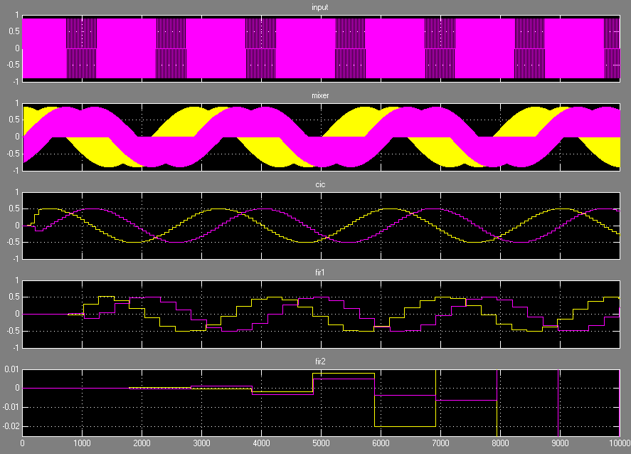
sim('demo_ddc', 550000.0*demo_ddc.SampleTime);Figure 43. Simulation Results Shown in the IScope BlockThe IScope block shows the first two channels (1 real and 1 complex for the first carrier) of data (magenta and yellow) as the input signals. The first trace shows the rapidly changing input signal that the testbench generates. The second signal shows the result of the mixer. This slowly changing signal contains the information to be extracted, plus a lot of high frequency residue. Applying the series of low-pass filters and decimating results in the required data.
 Note: If you turn on the Generate Hardware option in the parameters for the Control block, every time the simulation runs, DSP Builder synthesizes the underlying hardware, and writes out VHDL into the directory you specify.
 - Simulate the generated RTL in the ModelSim simulator.
- Synthesize and fit the RTL in the Quartus Prime software.