Video and Vision Processing Suite Intel® FPGA IP User Guide
A newer version of this document is available. Customers should click here to go to the newest version.
20.2. Full Raster to Clocked Video Converter Parameters
| Parameter | Values | Description |
|---|---|---|
| Video Data Format | ||
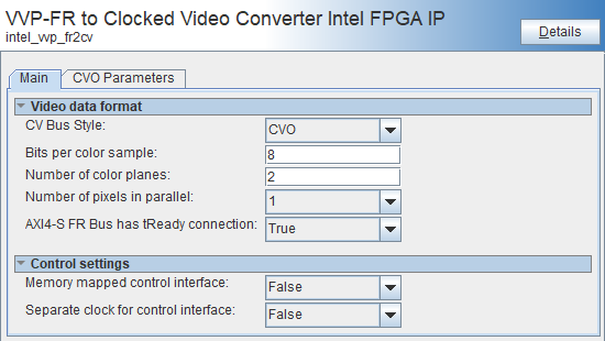
| CV Bus Style | Lite, CVI or CVO | Select which sideband signals the IP drives, and which signals are available in Platform Designer. A second tab allows configuration of the CV bus style. |
| Bits per color sample | 6 to 16 | Number of bits per color sample |
| Number of color planes | 1 to 4 | Number of color planes in a pixel |
| Number of pixels in parallel | 1, 2, 4 or 8 | Number of pixels transmitted every clock |
| AXI4S FR Bus has tReady connection | True or false | Select True so the full raster interface contains the AXI4-S tReady signal. Select False to remove the tReady signal. |
| Control Settings 49 | ||
| Memory-mapped control interface | True or false | Select True, to enable the CPU interface and associated signals. When False, the IP removes the CPU interface, and all CPU registers use default values. |
| Separate clock for control interface | True or false | Select True to include the signal cpu_clock to Platform Designer. You can assume it to be asynchronous to the video domain. When False, the CPU interface uses the signal vid_clock. |
| Parameters | Values | Description |
|---|---|---|
| Parameters | ||
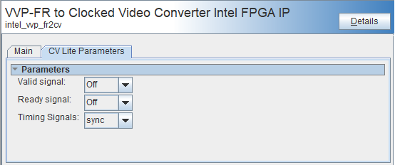
| Valid signal | On or off | When you select Lite the IP includes an optional data valid output signal, cv_vid_out_valid. Turn on to turn on this output in the IP. The Platform Designer GUI includes or removes the signal from the cv_vid_out conduit as appropriate. |
| Ready signal | On or off | When you select Lite, the IP includes an optional data ready input signal, cv_vid_out_ready. Turn on to turn on this input in the IP. Platform Designer includes or removes the signal from the cv_vid_out conduit as appropriate. |
| Timing signals | sync, blank, or both | Select which timing signals (blank timing or sync timing) are available. Platform Designer includes or removes the signals from the cv_vid_out conduit as appropriate |
| Parameter | Allowed Range | Description |
|---|---|---|
| CVI Core Parameters | ||
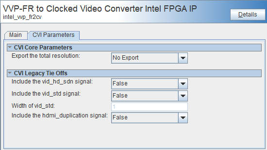
| Export the total resolution | No Export or Add signals for export | The dimensions of the full raster (active and blanking) can be output from the IP as 16-bit signals. Platform Designer includes or removes the signals from the cv_vid_out conduit as appropriate |
| CVI Legacy Tie Offs | ||
| Include the vid_hd_sdn signal | True or False | Select True to add this signal to the cv_vid_out conduit. The signal has no function within the IP and is included for connectivity within Platform Designer. |
| Include the vid_std signal | True or False | Select True to add this signal to the cv_vid_out conduit. The signal has no function within the IP and is included for connectivity within Platform Designer. |
| Width of vid_std | 1 to 16 | The width of the vid_std signal. |
| Include the hdmi_duplication signal | True or False | Select True to add this signal to the cv_vid_out conduit. The signal has no function within the IP and is included for connectivity within Platform Designer. |
| Parameters | Allowed Range | Description |
|---|---|---|
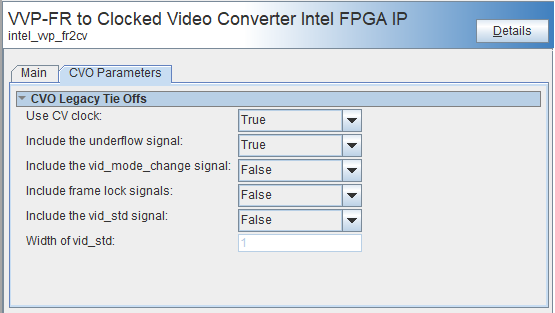
| CVO Legacy Tie Offs | ||
| Use CV Clock | True or False | Select True to add this signal to the cv_vid_out conduit. The clock signal is an input on the cv_vid_out conduit. If you select True, the IP uses it as the internal video clock. |
| Include the underflow signal | True or False | Select True to add this signal to the cv_vid_out conduit. The signal has no function within the IP and is included for connectivity within Platform Designer. |
| Include the vid_mode_change signal | True or False | Select True to add this signal to the cv_vid_out conduit. The signal has no function within the IP and is included for connectivity within Platform Designer. |
| Include the frame lock signals | True or False | Select True to add this signal to the cv_vid_out conduit. The signal has no function within the IP and is included for connectivity within Platform Designer. |
| Include the vid_std signal | True or False | Select True to add this signal to the cv_vid_out conduit. The signal has no function within the IP and is included for connectivity within Platform Designer. |
| Width of vid_std | 1 to 16 | The width of the vid_std signal. |