Video and Vision Processing Suite Intel® FPGA IP User Guide
ID
683329
Date
9/30/2022
Public
A newer version of this document is available. Customers should click here to go to the newest version.
1. About the Video and Vision Processing Suite
2. Getting Started with the Video and Vision Processing IPs
3. Video and Vision Processing IPs Functional Description
4. Video and Vision Processing IP Interfaces
5. Video and Vision Processing IP Registers
6. Video and Vision Processing IPs Software Programming Model
7. Protocol Converter Intel® FPGA IP
8. 3D LUT Intel® FPGA IP
9. AXI-Stream Broadcaster Intel® FPGA IP
10. Chroma Key Intel® FPGA IP
11. Chroma Resampler Intel® FPGA IP
12. Clipper Intel® FPGA IP
13. Clocked Video Input Intel® FPGA IP
14. Clocked Video to Full-Raster Converter Intel® FPGA IP
15. Clocked Video Output Intel® FPGA IP
16. Color Space Converter Intel® FPGA IP
17. Deinterlacer Intel® FPGA IP
18. FIR Filter Intel® FPGA IP
19. Frame Cleaner Intel® FPGA IP
20. Full-Raster to Clocked Video Converter Intel® FPGA IP
21. Full-Raster to Streaming Converter Intel® FPGA IP
22. Generic Crosspoint Intel® FPGA IP
23. Genlock Signal Router Intel® FPGA IP
24. Guard Bands Intel® FPGA IP
25. Interlacer Intel® FPGA IP
26. Mixer Intel® FPGA IP
27. Pixels in Parallel Converter Intel® FPGA IP
28. Scaler Intel® FPGA IP
29. Stream Cleaner Intel® FPGA IP
30. Switch Intel® FPGA IP
31. Tone Mapping Operator Intel® FPGA IP
32. Test Pattern Generator Intel® FPGA IP
33. Video Frame Buffer Intel® FPGA IP
34. Video Streaming FIFO Intel® FPGA IP
35. Video Timing Generator Intel® FPGA IP
36. Warp Intel® FPGA IP
37. Design Security
38. Document Revision History for Video and Vision Processing Suite User Guide
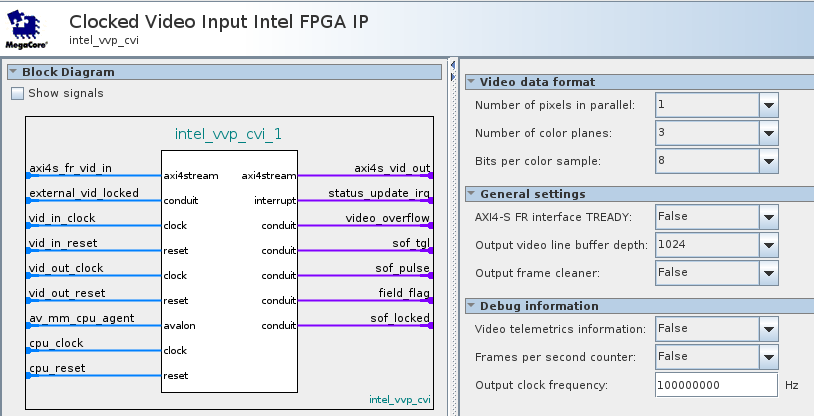
13.3. Clocked Video Input IP Parameters
The IP offers compile-time parameters.
| Parameter | Values | Description |
|---|---|---|
| Video Format | ||
| Bits per color sample | 8 to 16 | Select the number of bits per color sample at the input |
| Number of pixels in parallel | 1 to 8 | Select the number of pixels transmitted every clock cycle. |
| Number of color planes | 1 to 4 | Select the number of color planes per pixel |
| General Settings | ||
| AXI4-S FR interface TREADY | True or false | Enable the TREADY signal as part of the full-raster interface |
| Output video line buffer depth | 1024, 2048, 4096, 8192, 16384, 32768 | Select the maximum depth of the output video line buffer |
| Output frame cleaner | True or false | Enable the output frame cleaner logic |
| Debug Information | ||
| Video telemetrics information | True or false | Enable the video telemetrics information logic |
| Frames per second counter | True or false | Enable the frames per second counter logic |
| Output clock frequency | 1 to 1000000000 | Select the output clock frequency in Hz |
Figure 28. Clocked Video Input IP GUI