Intel® Arria® 10 Hard Processor System Technical Reference Manual
A newer version of this document is available. Customers should click here to go to the newest version.
7. SoC Security
The Intel® Arria® 10 SoC provides the framework for implementing secure systems by offering a layered hardware and software solution. A dedicated Security Manager module in the Hard Processor System (HPS) supervises secure initialization of the SoC and manages system response during tamper events. User fuses offer secure boot options and registers within the Security Manager provide further enhancement of secure states. Using Elliptical Curve Digital Signal Algorithm (ECDSA256) with Secure Hash Algorithm (SHA256) and Advanced Encryption Standard (AES) algorithms in the FPGA's Configuration Subsystem (CSS), boot images can be authenticated and decrypted. The integration of the Arm* TrustZone* technology and security firewalls within the Intel® Arria® 10 system interconnect provides defined partitioning in the device for secure and non-secure accesses. Protection mechanisms are integrated into debug components of the SoC to allow varying levels of visibility for debug.
Security Manager
The Security Manager module is integrated in the Hard Processor System (HPS) and provides the overall management of security within the SoC, including:
- Recognition of secure fuse configuration
- Secure state control and status check of security features
- Secure boot options
- Varying levels of debug visibility
- Anti-Tamper support
Security Manager Block Diagram
Functional Overview
The Security Manager integrates several functions that support the TrustZone* technology, manage security states in the device, and hold secure fuse information.
The main components of the Security Manager architecture include:
- Fuse Control (TEST):
When the HPS is powered, the Security Manager ensures reliable and verified receipt of the fuse information from the Configuration Subsystem (CSS) in the FPGA, stores it in fuse shadow registers and can request further fuse information.
- Security State and Status Check:
This sub-module holds the security state of the system, which is controlled by the fuse bits, hardware and software programming. This sub-module also has the ability to check and raise the level of security.
- Encryption Data Port:
This interface receives authenticated and decrypted boot images from the CSS.
- Support for ECDSA256 (SHA256) authenticated boot.
- Support for AES-based encrypted boot.
- Registers:
- Control Registers configure security state and debug options for the device.
- Status and Error Registers flag transmission errors and interrupts.
- Fuse Shadow Registers hold a copy of the user fuse information.
- Anti-Tamper Control:
On a tamper event, this module sends a signal to the Reset Manager to initiate the scrambling and clearing of all memories, including on-chip RAM, peripheral memories, L1 cache and L2 cache. Upon completion, the Security Manager sends a signal to the FPGA to indicate that the anti-tamper event has been handled.
Functional Description
Secure Initialization Overview
Secure initialization allows the device to boot and configure in a secured state.
Secure initialization begins with the CSS module. On FPGA power-up, the Configuration Subsystem (CSS) powers, initializes and loads the fuse bits. The CSS sends the FPGA its fuse configuration information. If the HPS is powered, the CSS sends the HPS fuse information to the Security Manager. This information is held in the HPS_fusesec shadow register in the Security Manager.
When the Security Manager is released from reset, it requests configuration information from the CSS and performs security checks. At this point, the rest of the HPS is still in reset. The security checks validate whether the state of each security option is valid. The Security Manager decodes the fuse bits and brings the rest of the HPS out of reset.
If there are errors in the initial transmission of the secure fuse information, the HPS stays in reset and no automatic retry occurs. Only an FPGA re-configuration causes a retry.
When the HPS is released from reset, the Security Manager sends signals to initialize the system blocks, such as the Clock Manager, FPGA Manager, System Manager. The clock control fuse information is automatically sent to the Clock Manager, the memory control fuse information is automatically sent to the Reset Manager and all other fuse functions (authentication, encryption, and public key source and length) are stored in a memory-mapped location for the boot ROM code to read. After these tasks are successfully completed, CPU0 comes out of reset in a secure state.
After CPU0 is released from reset, the boot ROM begins executing. At this time, the HPS is in a trusted state and the boot ROM code is guaranteed to execute as expected. For both secure and non-secure boot, all slave peripherals are brought out of reset in a secure state.
After initial security controls have been set, the boot ROM determines the second-stage boot loader source from the bootinfo register in the System Manager. The boot source can be from external memory through the HPS or through the FPGA. If the second-stage boot loader code comes from HPS external memory, then the boot ROM configures the clock and the interface to external memory.
When the boot ROM attempts to read from the flash, it looks for one of four images in external memory. Initially, it looks for image 0. If it is found, the image is authenticated, decrypted, or both depending on the requirements of the current security state. If these steps are successful, then the image is executed. However, if any of these steps fail, then the boot ROM moves onto the next image until it runs out of images.
For example, during a secure boot, the second-stage boot loader header includes an authentication key and the incoming image is authenticated. If indicated from the current security state, the image may be decrypted as well. The boot ROM contains functions to establish transitive trust to the second-stage boot code loaded from external flash or from the FPGA into on-chip RAM. If trust cannot be established in a secure boot, the HPS does not come out of reset and can attempt to load a different second-stage boot image.
For comprehensive information on the booting and boot image partitioning refer to the Booting and Configuration appendix of the Arria 10 Hard Processor Technical Reference Manual.
If all the images fail, it attempts to locate an image from the FPGA fabric and boot from there. If the FPGA boot fails, then it halts.
If the HPS receives its second-stage boot loader code from the FPGA, it waits for the FPGA to finish configuration before it obtains the image from FPGA RAM.
If required, a portion of the second-stage boot loader header can be used to raise security states of security features in the device that are currently in non-secure mode.
Secure Fuses
The following table details the HPS security fuse bits sent by the CSS to the Security Manager and contained within the HPS_fusesec register. A "blown" fuse state is represented by a 1 in the HPS_fusesec register and a "not blown" fuse state is represented by a 0.
| Bits |
Name | Description |
|---|---|---|
| 31:27 | Reserved | Bit values in this field are undefined. |
| 26:23 | csel_f | This field indicates the value of the clock select fuses that are available for configuring the clock for the boot interface and for the PLLs. Refer to the Clock Configuration section for more information on CSEL encodings. |
| 22 | dbg_access_f | This fuse determines the initial state of the debug access domains. |
| 21 | dbg_lock_JTAG | This field indicates if the HPS JTAG access level can be changed through software when the HPS is released from reset.
|
| 20 | dbg_lock_DAP | This field indicates if the DAP access level can be changed through software when the HPS is released from reset.
|
| 19 | dbg_lock_CPU0 | This field indicates if the CPU0 debug access level can be changed through software when the HPS is released from reset.
|
| 18 | dbg_lock_CPU1 | This field indicates if the CPU1 debug access level can be changed through software when the HPS is released from reset.
|
| 17 | dbg_lock_CS | This field indicates if the CoreSight debug access level can be changed through software when the HPS is released from reset.
|
| 16 | dbg_lock_FPGA | This field indicates if the FPGA debug access level can be changed through software when the HPS is released from reset.
|
| 15:12 | Reserved | Bit values in this field are undefined. |
| 11 | clr_ram_order_f | This fuse value determines how RAMs are cleared during a tamper event.
|
| 10 | clr_ram_cold_f | This fuse value indicates what happens to the RAM on a cold reset.
|
| 9 | clr_ram_warm_f | This fuse value indicates what happens to the RAMs on a warm reset.
|
| 8 | oc_boot_f | This fuse value determines if the second-stage boot code is allowed to boot from on-chip RAM.
|
| 7 | hps_clk_f | This fuse value selects the clock used for the boot process and in the case of a tamper event, memory scrambling.
|
| 6 | fpga_boot_f | If blown, this fuse value allows the FPGA to configure independently and allows the HPS to boot from an encrypted next-stage boot source that was decrypted into the FPGA.
|
| 5 | aes_en_f | This fuse value indicates if a decryption of the flash image is always performed.
|
| 4:2 | kak_src_f | This bit field indicates the source of the Key Authorization Key (KAK) which can be in:
|
| 1 | kak_len_f | This fuse value indicates the Key Authorization Key (KAK) length:
|
| 0 | authen_en_f | This fuse value determines whether authentication of flash images is required prior to execution.
|
At initialization, the FPGA also receives fuse information that is pertinent to its configuration. The HPS can read this information through a secure serial interface, which shifts the FPGA fuse values into the fpga_fusesec register in the Security Manager. The CSS shifts in a 32-bit value although some of the bits are considered reserved.
Security State
Each feature's security level can be increased from its initial fuse level through software, and for debug, through hardware as well. Changes to security level can only increase security and can never lower security. Both the HPS and FPGA have a mechanism to load security option bits as part of the second-stage boot loader and POF file, respectively, which can perform a check of the current security state and raise the security level.
Security Check
The Security Manager has the capability to perform security checks to identify discrepancies between the actual and expected security level so that measured actions can be taken through software and hardware if required.
- A fuse security level check
- A hardware access security level check
- A software access security level check
Secure Serial Interface
The HPS and FPGA communicate through a secure serial interface. The interface allows security of the HPS to be separate from the security of the FPGA. Software can initiate a request of the serial fuse interface via the Security Manager register.
Secure Debug
Debug logic in the Security Manager controls whether to enable or disable the JTAG, CPUs, Debug Access Port (DAP) and CoreSight* domains. Debug access is determined by a combination of debug fuses, option bits, and registers that change the default state and set the functional state of debug peripherals.
During a power-on reset, access to all debug domains are prevented. During a warm reset, access to all debug domains except JTAG are prevented. Once a cold or warm reset is exited, the default debug access is defined by the value of the dbg_disable_access fuse and the dbg_lock* fuses. When the dbg_disable_access fuse is blown, HPS debug accesses to all domains are disabled by default out of reset. If the fuse is not blown, then the initial HPS debug state out of reset is enabled. To ensure that the device is brought up in a secure state, the dbg_disable_access fuse must be blown.
MPU
The MPU supports invasive and non-invasive debug. Invasive debug allows the user to control and observe the processor. Non-invasive debug allows you to observe the processor but not control it and is always available as part of invasive debug. The NIDEN and SPNIDEN signals are used for non-invasive debug in the MPU.
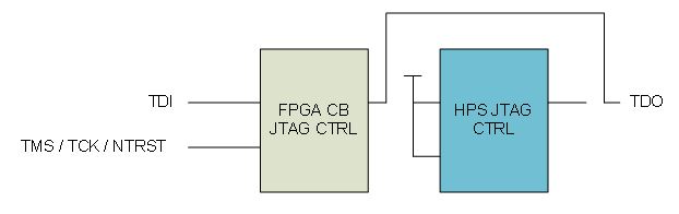
JTAG
The HPS and FPGA share a common set of JTAG pins and each have their own TAP controller which are chained together inside the device.
In the default JTAG configuration, the FPGA and HPS JTAG controllers are daisy-chained and controlled by an external JTAG port. The HPS JTAG controller is also referred to as the Debug Access Port.
Reset Manager
To avoid unsecure snooping of RAM contents, the Security Manager can send signals to the Reset Manager to clear all RAM on a cold or warm reset.
These signals are the result of fuse programming combined with the configuration bits found in the HPS_Swoptset and HPS_secopt1 register in the Security Manager.
In addition, the fuse information that determines whether the RAMs are cleared in series or parallel is also sent to the Reset Manager. Clearing the memory in series prevents a power spike that could occur with parallel clearing of RAM. The policies for how or when security states take affect can be programmed in the HPS_secopt1 register. Refer to the "Security State" section for more information.
The RAM instances that are cleared during a warm or cold reset are:
- On-chip RAM
- USB0
- USB1
- SD/MMC
- EMAC0 RX and TX buffer
- EMAC1 RX and TX buffer
- EMAC2 RX and TX buffer
- DMA
- NAND read data, write data, and ECC RAMs
- QSPI
- MPU RAM
If a tamper event occurs, the Security Manager notifies the Reset Manager and the following sequence occurs:
- All domain resets are asserted.
- All RAMs are cleared.
- The Reset Manager enters a dead state waiting for a POR release from Security Manager. All cold reset sources except Security Manager are ignored.
When FPGA POR and HPS POR are asserted, the Security Manager goes into reset.
Clock Configuration
Security Manager is driven by an internal oscillator, cb_intosc_hs_clk, in the Configuration Subsystem. This clock has wide variation across process and temperature. Once the Security Manager reads the fuse information, it drives the boot clock configuration to the Clock Manager. The Clock Manager samples the clock configuration on a cold and warm reset. If the hps_clk_f fuse is blown, the internal oscillator divided by 2, cb_intosc_hs_div2_clk, is used as the boot clock. If the fuse is not blown, an external oscillator is used. During boot ROM execution, the boot code configures the device clock based on the CSEL fuse settings or software code. The cb_intosc_hs_div2_clk can be considered the secure reference clock option.
The CSEL fuse settings have different meanings depending on how the hps_clk_f fuse is configured. When the hps_clk_f fuse is not blown, the external oscillator is the boot clock input.
| CSEL[3:0] Fuse Value |
Description |
MPU Clock Value |
|---|---|---|
| 0x0 | When no fuses are blown, the boot ROM returns clocks back to their default (bypass) boot mode and the CPU is driven by the external oscillator (HPS_CLK1), which must be in the range of 10 to 50 MHz. No PLL is enabled. | External Oscillator, HPS_CLK1 (10 to 50 MHz) |
| 0x1 | This encoding is typically used during a warm reset if you have already configured your clocks or PLL in the clock manager and would like to continue to use this configuration. If this is encoding is selected, no changes are made to these settings and the clock configuration is essentially user selected. If this is encoding is used during a power-on reset, then whatever the default reset values of the clocks are used. |
User-selected clock source. Refer to the Clock Manager chapter for clock register settings. |
| 0x2 | Reserved | External Oscillator, HPS_CLK1 (10 to 50 MHz) |
| 0x3 | Reserved | External Oscillator, HPS_CLK1 (10 to 50 MHz) |
| 0x4 | Reserved | External Oscillator, HPS_CLK1 (10 to 50 MHz) |
| 0x5 | Reserved | External Oscillator, HPS_CLK1 (10 to 50 MHz) |
| 0x6 | Reserved | External Oscillator, HPS_CLK1 (10 to 50 MHz) |
| 0x7 | External oscillator input clock, HPS_CLK1, is in the range of 10 to 15 MHz | 533 to 800Mhz |
| 0x8 | External oscillator input clock, HPS_CLK1, is in the range 15 to 20 MHz. | 600 to 800Mhz |
| 0x9 | External oscillator input clock, HPS_CLK1, is in the range 20 to 25 MHz. | 640 to 800Mhz |
| 0xA | External oscillator input clock, HPS_CLK1, is in the range 25 to 30 MHz. | 666 to 800Mhz |
| 0xB | External oscillator input clock, HPS_CLK1, is in the range 30 to 35 MHz. | 685 to 800Mhz |
| 0xC | External oscillator input clock, HPS_CLK1, is in the range 35 to 40 MHz. | 700 to 800Mhz |
| 0xD | External oscillator input clock, HPS_CLK1, is in the range 40 to 45 MHz. | 711 to 800Mhz |
| 0xE | External oscillator input clock, HPS_CLK1, is in the range 45 to 50 MHz. | 720 to 800Mhz |
| 0xF | The boot ROM returns clocks back to their default (bypass) boot mode and the CPU is driven by the external oscillator (HPS_CLK1). No PLL is enabled. | External Oscillator, HPS_CLK1 (10 to 50 MHz) |
| CSEL[3:0] Fuse Value |
Description |
MPU Clock Value |
|---|---|---|
| 0x0 | Bypass mode; in this mode all clocks are reset and boot mode is ensured active; cb_intosc_hs_div2_clk (cb_intosc_hs clock divided by 2) is used. | cb_intosc_hs_div2_clk (60 to 200 MHz) |
| 0x1 | This encoding is typically used during a warm reset if you have already configured your clocks or PLL in the Clock Manager and would like to continue to use this configuration. If this is encoding is selected, no changes are made to these settings and the clock configuration is essentially user selected. If this is encoding is used during a power-on reset, then whatever the default reset values of the clocks are used. |
User-selected clock source. Refer to the Clock Manager chapter for clock register settings. |
| 0x2 | PLL is used with the internal oscillator (30 to 100 MHz) | 120 to 800 MHz |
| 0x3 | Reserved | cb_intosc_hs_div2_clk (60 to 200 MHz) |
| 0x4 | Reserved | cb_intosc_hs_div2_clk (60 to 200 MHz) |
| 0x5 | Reserved | cb_intosc_hs_div2_clk (60 to 200 MHz) |
| 0x6 | Reserved | cb_intosc_hs_div2_clk (60 to 200 MHz) |
| 0x7 | Reserved | cb_intosc_hs_div2_clk (60 to 200 MHz) |
| 0x8 | Reserved | cb_intosc_hs_div2_clk (60 to 200 MHz) |
| 0x9 | Reserved | cb_intosc_hs_div2_clk (60 to 200 MHz) |
| 0xA | Reserved | cb_intosc_hs_div2_clk (60 to 200 MHz) |
| 0xB | Reserved | cb_intosc_hs_div2_clk (60 to 200 MHz) |
| 0xC | Reserved | cb_intosc_hs_div2_clk (60 to 200 MHz) |
| 0xD | Reserved | cb_intosc_hs_div2_clk (60 to 200 MHz) |
| 0xE | Reserved | cb_intosc_hs_div2_clk (60 to 200 MHz) |
| 0xF | Bypass mode; reset all clocks and ensure boot mode is active; cb_intosc_hs_div2_clk is used. | cb_intosc_hs_div2_clk (60 to 200 MHz) |
For more information regarding the CSEL encodings and descriptions, please refer to the Booting and Configuration Appendix.
FPGA Security Features
The FPGA has several security fuses which can control the following functions:
- Limiting acceptance of only encrypted and authenticated POFs
- Disabling partial reconfiguration and scrubbing
- Disabling test access
- Disabling external configuration
- Limiting JTAG access
- Bypassing HPS or FPGA JTAG
- Locking or disabling the battery-backed volatile key
- Disabling the OTP key
Note that there is a fuse sent to the FPGA CSS, called hps_jtag_bypass, which performs the same function of removing the HPS from the JTAG chain. However, this fuse is a permanent disable, whereas using software to program the sec_jtagdbg register has the same affect, but may be changed later by software.
Secure Boot
No ordering of boot or FPGA configuration is required because the FPGA and HPS may be brought up in any order, and they can both raise the security level of the entire device at any time before user code is loaded to execute.
The SoC may securely boot in one of three ways:
- The HPS boot and FPGA configuration occur separately.
- The HPS boots from the FPGA after the FPGA is configured
- The HPS boots first and configures the FPGA.
Boot Configuration
Booting configuration is provided from a combination of the BSEL pins and the boot mode fuses. The BSEL pins indicate if the boot source is the FPGA or one of the HPS flash interfaces. If the fpga_boot_f fuse is blown, it overrides these pin values. The fpga_boot_f fuse value can be read from the hps_fusesec register.
| BOOTSEL Field Value |
Flash Device |
|---|---|
| 0x0 |
Reserved |
| 0x1 |
FPGA (HPS-to-FPGA bridge) |
| 0x2 |
1.8 V NAND flash memory |
| 0x3 |
3.0 V NAND flash memory |
| 0x4 |
1.8 V SD/MMC flash memory with external transceiver |
| 0x5 |
3.0 V SD/MMC flash memory with internal transceiver |
| 0x6 |
1.8 V quad SPI flash memory |
| 0x7 |
3.0 V quad SPI flash memory |
Within the device, there are fuses that provide some of the boot mode configuration information. The fuse values can be read through the HPS_fusesec register:
| Bits |
Name | Description |
|---|---|---|
| 31:27 | Reserved | Bit values in this field are undefined. |
| 26:23 | csel_f | This field indicates the value of the clock select fuses that are available for configuring the clock for the boot interface and for the PLLs. Refer to the Clock Configuration section for more information on CSEL encodings. |
| 22 | dbg_access_f | This fuse determines the initial state of the debug access domains. |
| 21 | dbg_lock_JTAG | This field indicates if the HPS JTAG access level can be changed through software when the HPS is released from reset.
|
| 20 | dbg_lock_DAP | This field indicates if the DAP access level can be changed through software when the HPS is released from reset.
|
| 19 | dbg_lock_CPU0 | This field indicates if the CPU0 debug access level can be changed through software when the HPS is released from reset.
|
| 18 | dbg_lock_CPU1 | This field indicates if the CPU1 debug access level can be changed through software when the HPS is released from reset.
|
| 17 | dbg_lock_CS | This field indicates if the CoreSight debug access level can be changed through software when the HPS is released from reset.
|
| 16 | dbg_lock_FPGA | This field indicates if the FPGA debug access level can be changed through software when the HPS is released from reset.
|
| 15:12 | Reserved | Bit values in this field are undefined. |
| 11 | clr_ram_order_f | This fuse value determines how RAMs are cleared during a tamper event.
|
| 10 | clr_ram_cold_f | This fuse value indicates what happens to the RAM on a cold reset.
|
| 9 | clr_ram_warm_f | This fuse value indicates what happens to the RAMs on a warm reset.
|
| 8 | oc_boot_f | This fuse value determines if the second-stage boot code is allowed to boot from on-chip RAM.
|
| 7 | hps_clk_f | This fuse value selects the clock used for the boot process and in the case of a tamper event, memory scrambling.
|
| 6 | fpga_boot_f | If blown, this fuse value allows the FPGA to configure independently and allows the HPS to boot from an encrypted next-stage boot source that was decrypted into the FPGA.
|
| 5 | aes_en_f | This fuse value indicates if a decryption of the flash image is always performed.
|
| 4:2 | kak_src_f | This bit field indicates the source of the Key Authorization Key (KAK) which can be in:
|
| 1 | kak_len_f | This fuse value indicates the Key Authorization Key (KAK) length:
|
| 0 | authen_en_f | This fuse value determines whether authentication of flash images is required prior to execution.
|
Secure Boot Process
Secure boot allows the HPS to release from reset into a known state and then validate the authenticity and integrity of the second-stage boot loader code prior to executing it. Secure boot ensures that only authorized code is executed on the system. In addition, the system has the option to configure the FPGA from the HPS, which provides a secure boot mechanism for the FPGA portion of the SoC. In this mode, the HPS boot code can authenticate the FPGA POF prior to loading it.
The HPS and FPGA can also be booted securely but independently, with the HPS executing authenticated and decrypted user code out of external RAM and the FPGA receiving an encrypted FOP configuration file by enabling an FPGA configuration source through the MSEL pins.
Boot ROM code runs on CPU0 and CPU1 is held in reset. Once control passes to the second-stage boot loader, CPU1 can be released from reset.
Authentication and Decryption
Authentication is provided for the second-stage boot loader code and both the HPS and FPGA can utilize the AES algorithms in the Configuration Subsystem (CSS) to decrypt boot images and POF files, respectively.
Three levels of boot are available to the device:
- Authentication only: The second-stage boot loader code is not encrypted, but there are public key signatures attached to the image and the code only executes if all of the signatures pass. ECDSA256 (SHA 256) is used for authenticated boot.
- Decryption only: The user boot code is encrypted and must be decrypted before execution. AES-based algorithms in the FPGA are used for decryption.
- Authentication and Decryption: The user boot code is encrypted and signed.
If authentication and decryption are enabled, the data is first authenticated and then decrypted using the AES algorithms. Authentication is performed using the public key authorization key (KAK) held in the user fuses. The KAK can be 256 bits. The KAK public key authentication fuses are lockable by the user in groups of 64 bits or less.
The Security Manager's hps_fusesec register can be read to identify the source of the public (root) key used for authentication of the second-stage boot loader. The source of the public (root) key can be one of the following:
- External software
- ROM
- FPGA logic elements
- User Access Fuses (UAF)
AES decryption algorithms are available through the FPGA CSS and are enabled prior to decryption through a combination of user fuses and software programming. Elliptic curve cryptographic algorithms are used in an authenticated boot. Decrypted data is sent to the Security Manager to be read by the CPU or DMA.
The FPGA has higher priority in the CSS, and the FPGA AES algorithms abort decryption and authentication of data if the FPGA starts configuration or reconfiguration.
Anti-Tamper
The Security Manager receives a tamper detection signal when a tamper event is detected in the device.
Anti-tamper logic can be implemented in the FPGA soft logic to detect a tamper event. No tamper detection is available until the FPGA is configured. The user must define the anti-tamper design. Some examples of tamper detection that could be implemented are:
- Using the FPGA voltage sensor to detect any IR drops across the device.
- Using an A/D controller to detect temperature changes in the device due to tamper.
- Assigning loaner I/O as dedicated tamper pins to detect package break-away.
The tamper detection signal sent to the Security Manager, anti_tamper_in, is an active low signal. When there is no tamper event, it is driven to 1. The Security Manager also provides a tamper acknowledge signal to the FPGA interface. The tamper event input to the HPS is gated with a signal indicating the completion of FPGA configuration. This prevents an inadvertent tamper event assertion or tamper response from the HPS to the rest of the system.
- Ethernet MAC 0/1/2
- USB OTG 0/1
- QSPI flash controller
- NAND flash controller
- SD/MMC controller
- DMA controller
Upon completion of memory scrambling of all IPs, the Security Manager sends a response to the FPGA indicating that a tamper event has been handled in the HPS. This response is followed by HPS entering into a cold reset without exiting until another power cycle occurs. Both Security Manager and Reset Manager enter reset. Other resets, such as warm reset or cold reset, do not affect the state of the Security Manager or the Reset Manager.
If the FPGA POR is de-asserted while the HPS is in a tamper event reset, then the Security Manager goes back to the reset state.
Security System Extensions
Beyond the Security Manager module, other secure features can be implemented at a system level within the SoC.
TrustZone
TrustZone* security is implemented in the Cortex*-A9 MPU subsystem in three ways:
- Hardware partitioning through the implementation of firewalls: Resources can be assigned and identified as secure or non-secure.
- Virtual processor execution: Each core can context switch between secure and non-secure operation.
- Secure debug control: Both secure and non-secure hardware debug exist and the type of debug allowed can be configured by the user.
Secure Partitioning
System interconnect and cache accesses as well as processor execution can be securely partitioned using the TrustZone* infrastructure.
Secure Bus Accesses
The Cortex* -A9 MPCore and other masters that utilize the system interconnect can be configured for secure or non-secure accesses.
Master accesses drive a protection signal, AxPROT[1], to communicate the security level of the attempted transaction. The Cortex* -A9 drives this signal low for secure accesses and high for non-secure accesses. The secure firewalls determine whether the access is allowed or not. A slave access type defaults to secure if no other configuration is programmed. Users can define whether a bus error is generated or if a bus failure occurs when a secure access is violated.
Secure Cache Accesses
Secure and non-secure partitioning also extends to the L1 and L2 caches.
There is a 32-bit physical address space for secure and non-secure transactions and a 33rd bit is provided to indicate security. The cache is able to store both secure and non-secure lines.
The Accelerator Coherency Port (ACP) in the Arm* Cortex* -A9 MPCore can be used with TrustZone* technology. The security state of the masters using the ACP must be the same as the Cortex-A9 processor.
Virtual Processor Operation
Two virtual processors (secure and non-secure) with context switch capability (monitor mode) exist for each Cortex*-A9 processor core. The secure virtual processor only accesses secure resources and the non-secure virtual processor only accesses non-secure resources.
Exception Vector Tables
A context switch to secure operation is achieved through a secure monitor call (SMC) instruction or the following hardware exceptions (if configured to do so):
- IRQ interrupt
- Faster Interrupt Request (FIQ) interrupt
- External data abort
- External prefetch abort
When a context switch occurs, the state of the current mode is saved and restored on the next context switch or on a return from exception.
Three exception vector tables are provided for the MPU with TrustZone* :
- Non-secure
- Secure
- Monitor mode
Typically IRQs are used for non-secure interrupts and FIQs are used for secure interrupts. The location of each of the three vector tables can be moved at runtime.
The Generic Interrupt Controller (GIC) can handle secure and non-secure interrupts and prevent non-secure accesses from reading or modifying the configuration of a secure interrupt. An interrupt can be made secure by programming the appropriate bits in the Interrupt Security Register. Secure interrupts are always given a higher priority than non-secure interrupts.
Arria 10 HPS Secure Firewalls
You can use the system interconnect firewalls to enforce security policies for slave and memory regions in the system interconnect.
The firewalls support the following features:
- Secure or non-secure access configurable per peripheral
- Privileged or user access configurable for some peripherals
- Per-transaction security
There are five main firewalls in the HPS:
- Peripheral
- System
- HPS-to-FPGA
- On-Chip RAM
- SDRAM (which includes DDR and DDR L3 firewalls)
Firewall Diagrams
The system interconnect firewalls filter access to components on various buses.
| Name |
Function |
|---|---|
| Peripherals | The peripherals firewall filters access to slave peripherals in the following buses:
|
| System | The system firewall filters access to system peripherals in the following components:
|
| HPS-to-FPGA | The HPS-to-FPGA firewall filters access to FPGA through the following bridges:
|
| On-Chip RAM | The on-chip RAM firewall filters secure access to on-chip RAM |
| SDRAM | The SDRAM firewall filters access to DDR SDRAM |
| Bus Behind Firewall |
Bus Slaves Behind Firewall | Masters That Can Access Bus |
|---|---|---|
| L4 Main |
DMA (secure/non-secure registers) SPI 0/1/2/3 |
MPU DAP DMA FPGA-to-HPS |
| L4 Master Peripheral Bus |
EMAC 0/1/2 SD/MMC QSPI |
MPU DAP DMA FPGA-to-HPS |
| L4 AHB* Bus |
QSPI Data NAND Data USB OTG 0/1 |
MPU DAP DMA FPGA-to-HPS |
| L4 Slave Peripheral Bus |
UART 0/1 I2C 0/1/2/3/4 SP Timer 0/1 GPIO 0/1/2 |
MPU DAP DMA FPGA-to-HPS |
| Bus Behind Firewall |
Bus Slaves Behind Firewall | Masters That Can Access Bus |
|---|---|---|
| L4 ECC |
SD/MMC ECC DMA ECC QSPI ECC NAND ECC USB 0/1 ECC On-Chip RAM ECC EMAC 0/1/2 Rx ECC EMAC 0/1/2 Tx ECC NAND Read/Write ECC |
MPU FPGA-to-HPS DAP |
| L4 System |
FPGA Manager Data and Registers OSC Timer 0/1 Watchdog 0/1 System Manager L3 Interconnect Control and Status Registers (CSR) L4 Interconnect firewall Security Control Registers (SCR) |
MPU FPGA-to-HPS DAP DMA |
| L4 DAP Bus |
STM DAP |
MPU FPGA-to-HPS DAP |
| Bus Behind Firewall |
Bus Slaves | Masters that can Access Bus |
|---|---|---|
| L3 |
SD/MMC ECC DMA ECC QSPI ECC NAND ECC USB 0/1 ECC On-Chip RAM ECC EMAC 0/1/2 Rx ECC EMAC 0/1/2 Tx ECC NAND Read/Write ECC |
MPU FPGA-to-HPS DAP |
| L4 System |
FPGA Manager Data and Registers OSC Timer 0/1 Watchdog 0/1 System Manager L3 Interconnect CSR L4 Interconnect firewall SCR |
MPU FPGA-to-HPS DAP DMA |
| L4 DAP Bus |
STM DAP |
MPU FPGA-to-HPS DAP |
Secure Transaction Protection
The interconnect provides two levels of transaction protection.
- Security Firewalls:
Security firewalls enforce the Secure World read and write transactions. The term "security firewall" and "firewall" may be used interchangeably within the context of this section.
- Privilege filter
The privilege filter leverages the firewall mechanism and provides additional filtering by allowing control of the privilege level of L4 slave transactions. The privilege filter applies to writes only.
All slaves on the SoC are placed behind a security firewall. A subset of slaves are also placed behind a privilege filter. Transactions to these slaves pass through two firewall structures as shown in the figure below. The transaction packet must pass both a security firewall and the privilege filter to reach the slave. A transaction error causes random data or a slave error depending on where the transaction failed and how the error_response bit in the global register of the noc_fw_ddr_l3_ddr_scr module is programmed.
Each firewall has an associated firewall register which can be programmed by the DAP, FPGA fabric or MPU in secure mode only. A subset of the L4 slaves can additionally be programmed to configure their privilege filter policy.
Peripheral and System Firewalls
The peripheral and system firewalls each have a group of Security Configuration Registers (SCRs) that can be programmed by the DAP, FPGA fabric or MPU only in secure mode.
| Secure Flag Value | Access |
|---|---|
| 0 | Only secure packets are allowed to pass the firewall. |
| 1 | Transaction packets are allowed to pass the firewall. |
When a transaction packet is sent from a master, the master also drives a secure flag signal on the bus. This flag indicates whether the attempted transaction from the master is secure or non-secure. For AXI master accesses, this flag is the ~AxPROT[1] signal.
For L4 ECC, L4 system or L4 DDR master accesses, this flag is the MSecure[0] signal.
When the flag signal is driven high, it indicates a secure access. When the flag signal is low, it indicates a non-secure access.
Secure Transaction Example
A successful secure access attempt by a master, depends on the security bit configuration in the Security Control Register and the value of the master secure flag sent by the master.
All SoC transactions are set to secure out of reset with a return of random data when transactions are blocked. If you want an error response returned for blocked transactions, you must set the error_response bit in the global register of the noc_fw_ddr_l3_ddr_scr module at base address 0xFFD13400. If this bit is clear, transactions blocked by the firewall return random data.
To initiate a secure transaction:
- The master drives the address of the slave as well as the master secure flag signal, indicating that the access is intended to be secure.
- The firewall compares the programmed security bit of the master-slave peripheral pair to the master secure flag signal to determine if the access is valid.
- If the access is valid, the transaction passes to the next level. If the access is not valid, random data is fed back to the master.
| Security Bit in Firewall Register |
Master Secure Flag |
Transaction Pass/Fail | Transaction Type |
|---|---|---|---|
| 0 |
0 |
No | None (Blocked transaction) |
| 0 |
1 |
Yes | Secure |
| 1 |
0 |
Yes | Non-secure |
| 1 |
1 |
Yes | Secure |
Non-secure Transaction Configuration
When the SoC is released from reset, only secure transactions are allowed through the firewalls. The user must configure any master-slave pairs that are required to be non-secure.
- After the SoC is released from reset, the MPU, FPGA2SOC masters or the DAP accesses the required Security Configuration Register (SCR) by executing a secure write. The peripheral firewall SCR registers are within the soc_noc_fw_l4_per register group and the system firewall SCR registers are found within the soc_noc_fw_l4_sys register group.
- To configure the slave to allow a non-secure access by a master, set the corresponding security bit to 1.
HPS-to-FPGA Firewall
The HPS-to-FPGA firewall is used to filter access to all the FPGA, including the HPS-to-FPGA bridge and the lightweight HPS-to-FPGA bridge.
On-Chip RAM Firewall
At reset all memories are secure. Out of reset, regions of memories can be configured for non-secure accesses.
The on-chip RAM is divided into six regions, where the granularity of the address boundary is 4 KB. Within each region, a non-secure or shared memory region can be assigned by programming a base and limit value in the corresponding regionNaddr register, with N denoting the region number. Each of these regions can be enabled by writing to the enable register or setting the corresponding bit in the enable_set register.
When an incoming transaction falls within any enabled non-secure regions, the firewall allows both secure and non-secure packets. When the transaction is outside of any enabled regions, the firewall only allows secure packets.
When a transaction packet is sent from a master, the master also drives a secure master flag signal on the bus. This flag indicates whether the attempted transaction from the master is for a secure or non-secure memory region. When the flag signal is driven high, it indicates a secure access. When the flag signal is low it indicates a non-secure access.
On-Chip RAM Transaction Configuration
Because all memories are secure when they exit reset, the on-chip RAM Security Control Register block must be configured by a secure master before non-secure or shared memory accesses are allowed.
- Configure the base and limit fields of the regionNaddr register, where N denotes the region number.
- Enable the non-secure memory region by setting the corresponding regionNenable bit in the enable_set register, where N denotes the region number.
SDRAM Firewall
Two SDRAM firewalls are implemented to allow a different security policy depending on the master.
One firewall filters accesses from the MPU and the FPGA-to-SDRAM interface. The other firewall filters accesses from all other masters on the HPS and applies the same security policy to both coherent and non-coherent accesses. Both firewalls are logically and physically split within the interconnect.
The SDRAM Firewall supports a minimum region size of 64 KB. Each master is allowed a different number of firewall regions:
- The MPU can have up to four firewall regions.
- The FPGA-to-SDRAM interface can have up to twelve firewall regions.
- Any HPS bus master can have up to eight firewall regions.
Privilege Filter
If a transaction packet has passed the security firewall, it may pass through a privilege filter. The privilege filter only applies to writes. All reads are passed without exception.
The following slaves can be programmed using the privilege registers in the interconnect module:
- HPS-to-FPGA bridge
- Lightweight HPS-to-FPGA bridge
- UARTs
- SP Timers
- I2C Modules
- GPIO
- SD/MMC
- QSPI
- EMAC Modules
- SPI
- Secure and non-secure DMA
- USB
- NAND Controller
| Read/Write |
Privilege Signal |
Privilege bit | Transaction Pass/Fail |
|---|---|---|---|
| Read |
0 |
0 | Pass |
| 0 |
1 | Pass | |
| 1 |
0 | Pass | |
| 1 |
1 | Pass | |
| Write |
0 |
0 | Fail |
| 0 |
1 | Pass | |
| 1 |
0 | Pass | |
| 1 |
1 | Pass |
Master Security Policy
Each master has an inherent security transaction capability.
Masters accessing slaves can be configured to one of three different security policies:
- Per transaction: The master is capable of generating secure and non-secure transactions.
- Secure: The master only supplies secure transactions.
- Non-secure: The master only generates non-secure transactions.
| Master |
Transaction Capability |
|---|---|
| DMA |
Secure/Non-secure |
| DAP |
Secure/Non-secure |
| USB OTG 0/1 |
Non-secure |
| SD/MMC |
Non-secure |
| EMAC0/1/2 |
Secure/Non-secure |
| NAND |
Non-secure |
| FPGA-to HPS Bridge |
Secure/Non-secure |
| ETR |
Secure/Non-secure |
| MPU |
Secure/Non-secure |
| FPGA-to-SDRAM |
Secure/Non-secure |
Security policies are based on secure and privilege attributes. For instance, if CPU0 is configured to access NAND registers in both secure and non-secure mode and CPU0 attempts an access when the core is in secure or non-secure mode, no error occurs. However, if CPU0 is allowed to access NAND registers only in secure mode and CPU0 is operating in non-secure mode, then CPU0 receives an error response when accessing the NAND registers. If both the security firewall and privilege firewall are implemented, security firewall filters all of the accesses. If an access fails, random data or an error response is sent to the master, depending on how the error_response bit in the global register of the noc_fw_ddr_l3_ddr_scr module is programmed. If access is granted by the security firewall, then the transaction enters the privilege firewall. If access is granted, the request enters the peripheral IP.
Secure Interconnect Reset
When the SoC is released from reset, every slave on the interconnect is in the secure state (boot secure).
The only masters capable of secure accesses out of reset are:
- MPU
- DAP
- HPS-to-FPGA fabric