Intel® Arria® 10 Hard Processor System Technical Reference Manual
A newer version of this document is available. Customers should click here to go to the newest version.
15.4. Functional Description of the SD/MMC Controller
SD/MMC/CE-ATA Protocol
- Command—a token transmitted serially on the CMD pin that starts an operation.†
- Response—a token from the card transmitted serially on the CMD pin in response to certain commands.†
- Data—transferred serially using the data pins for data movement commands.†
In the following figure, the clock is a representative only and does not show the exact number of clock cycles.
The following figure illustrates an example of a command token sent by the host in a multiple‑block write operation.
BIU
- Slave interface
- Register block
- FIFO buffer
- Interrupt control
- Internal DMA controller
Slave Interface
Register Block
All registers reside in the BIU clock domain, l4_mp_clk. When a command is sent to a card by setting the start command bit (start_cmd) of the command register (cmd) to 1, all relevant registers needed for the CIU operation are copied to the CIU block. During this time, software must not write to the registers that are transferred from the BIU to the CIU. The software must wait for the hardware to reset the start_cmd bit to 0 before writing to these registers again. The register unit has a hardware locking feature to prevent illegal writes to registers.
Registers Locked Out Pending Command Acceptance
- Command (cmd)†
- Command argument (cmdarg)†
- Byte count (bytcnt)†
- Block size (blksiz)†
- Clock divider (clkdiv)†
- Clock enable (clkena)†
- Clock source (clksrc)†
- Timeout (tmout)†
- Card type (ctype)†
The hardware resets the start_cmd bit after the CIU accepts the command. If a host write to any of these registers is attempted during this locked time, the write is ignored and the hardware lock write error bit (hle) is set to 1 in the raw interrupt status register (rintsts). Additionally, if the interrupt is enabled and not masked for a hardware lock error, an interrupt is sent to the host.†
Once a command is accepted, you can send another command to the CIU—which has a one‑deep command queue—under the following conditions:†
- If the previous command is not a data transfer command, the new command is sent to the SD/MMC/CE‑ATA card once the previous command completes.†
- If the previous command is a data transfer command and if the wait previous data complete bit (wait_prvdata_complete) of the cmd register is set to 1 for the new command, the new command is sent to the SD/MMC/CE‑ATA card only when the data transfer completes.†
- If the wait_prvdata_complete bit is 0, the new command is sent to the SD/MMC/CE‑ATA card as soon as the previous command is sent. Typically, use this feature to stop or abort a previous data transfer or query the card status in the middle of a data transfer.†
Interrupt Controller Unit
The interrupt controller unit generates active high, level sensitive interrupts that are asserted only when at least one bit in the rintsts register is set to 1, the corresponding intmask register bit is 1, and the int_enable bit of the ctrl register is 1.
The int_enable bit of the ctrl register is cleared during a power-on reset, and the intmask register bits are set to 0x0000000, which masks all the interrupts.
| Bits | Interrupt | Description |
|---|---|---|
| 16 | SDIO Interrupts† | Interrupts from SDIO cards.† |
| 15 | End Bit Error (read)/Write no CRC (EBE)† | Error in end-bit during read operation, or no data CRC received during write operation.†
Note: For MMC CMD19, there may be no CRC status returned by the card. Hence, EBE is set for CMD19. The application should not treat this as an error. †
|
| 14 | Auto Command Done (ACD)† | Stop/abort commands automatically sent by card unit and not initiated by host; similar to Command Done (CD) interrupt. † Recommendation: Software typically need not enable this for non CE-ATA accesses; Data Transfer Over (DTO) interrupt that comes after this interrupt determines whether data transfer has correctly competed. For CE-ATA accesses, if the software sets send_auto_stop_ccsd bit in the control register, then software should enable this bit.† |
| 13 | Start Bit Error (SBE) | Error in data start bit when data is read from a card. In 4-bit mode, if all data bits do not have start bit, then this error is set. |
| 12 | Hardware Locked write Error (HLE)† | During hardware-lock period, write attempted to one of locked registers. † |
| 11 | FIFO Underrun/Overrun Error (FRUN)† | Host tried to push data when FIFO was full, or host tried to read data when FIFO was empty. Typically this should not happen, except due to error in software. † Card unit never pushes data into FIFO when FIFO is full, and pop data when FIFO is empty. † If IDMAC (Internal Direct Memory Access Controller) is enabled, FIFO underrun/overrun can occur due to a programming error on MSIZE and watermark values in FIFOTH register; for more information, refer to Internal Direct Memory Access Controller (IDMAC) section in the "Synopsys DesignWare Cores Mobile Storage Host Databook".† |
| 10 | Data Starvation by Host Timeout (HTO)† | To avoid data loss, card clock out (cclk_out) is stopped if FIFO is empty when writing to card, or FIFO is full when reading from card. Whenever card clock is stopped to avoid data loss, data-starvation timeout counter is started with data-timeout value. This interrupt is set if host does not fill data into FIFO during write to card, or does not read from FIFO during read from card before timeout period. † Even after timeout, card clock stays in stopped state, with CIU state machines waiting. It is responsibility of host to push or pop data into FIFO upon interrupt, which automatically restarts cclk_out and card state machines. † Even if host wants to send stop/abort command, it still must ensure to push or pop FIFO so that clock starts in order for stop/abort command to send on cmd signal along with data that is sent or received on data line. † |
| 9 | Data Read Timeout (DRTO)/Boot Data Start (BDS)† |
|
| 8 | Response Timeout (RTO)/ Boot Ack Received (BAR)† |
|
| 7 | Data CRC Error (DCRC)† | Received Data CRC does not match with locally-generated CRC in CIU; expected when a negative CRC is received. † |
| 6 | Response CRC Error (RCRC)† | Response CRC does not match with locally-generated CRC in CIU.† |
| 5 | Receive FIFO Data Request (RXDR)† | Interrupt set during read operation from card when FIFO level is greater than Receive-Threshold level.† Recommendation: In DMA modes, this interrupt should not be enabled.†
ISR, in non-DMA mode:
|
| 4 | Transmit FIFO Data Request (TXDR)† | Interrupt set during write operation to card when FIFO level reaches less than or equal to Transmit-Threshold level.† Recommendation: In DMA modes, this interrupt should not be enabled.† ISR in non-DMA mode: † |
| 3 | Data Transfer (DTO)† | Data transfer completed, even if there is Start Bit Error or CRC error. This bit is also set when “read data-timeout” occurs or CCS is sampled from CE-ATA device.† Recommendation: In non-DMA mode, when data is read from card, on seeing interrupt, host should read any pending data from FIFO. In DMA mode, DMA controllers guarantee FIFO is flushed before interrupt.†
Note: DTO bit is set at the end of the last data block, even if the device asserts MMC busy after the last data block.†
|
| 2 | Command Done (CD)† | Command sent to card and received response from card, even if Response Error or CRC error occurs. Also set when response timeout occurs or CCSD sent to CE-ATA device.† |
| 1 | Response Error (RE)† | Error in received response set if one of following occurs:†
|
| 0 | Card-Detect (CDT)† | When one or more cards inserted or removed, this interrupt occurs. Software should read card-detect register (CDETECT, 0x50) to determine current card status.† Recommendation: After power-on and before enabling interrupts, software should read card detect register and store it in memory. When interrupt occurs, it should read card detect register and compare it with value stored in memory to determine which card(s) were removed/inserted. Before exiting ISR, software should update memory with new card-detect value.† |
Interrupt Setting and Clearing
For example, on receiving the Receive FIFO Data Request interrupt, the FIFO buffer must be emptied so that the FIFO buffer count is not greater than the RX watermark, which causes the interrupt to be triggered.†
The rest of the interrupts are triggered by single clock‑pulse‑width sources.†
FIFO Buffer
The SD/MMC controller has a 4 KB data FIFO buffer for storing transmit and receive data.
The FIFO has an ECC controller built-in to provide ECC protection. The ECC controller is able to detect single-bit and double-bit errors, and correct the single-bit errors. The ECC operation and functionality is programmable through the ECC register slave interface. The ECC register slave interface provides host access to configure the ECC logic as well as inject bit errors into the memory. It also provides the host access to memory initialization hardware used to clear out the memory contents including the ECC bits. The ECC controller generates interrupts upon occurrences of single- and double-bit errors, and the interrupt signals are connected to the system manager.
Internal DMA Controller
- Supports 32-bit data
- Supports split, retry, and error AHB* responses, but does not support wrap
- Configurable for little-endian or big-endian mode
- Allows the selection of AHB* burst type through software
The internal DMA controller has a CSR and a single transmit or receive engine, which transfers data from system memory to the card and vice versa. The controller uses a descriptor mechanism to efficiently move data from source to destination with minimal host processor intervention. You can configure the controller to interrupt the host processor in situations such as transmit and receive data transfer completion from the card, as well as other normal or error conditions. The DMA controller and the host driver communicate through a single data structure.†
The internal DMA controller transfers the data received from the card to the data buffer in the system memory, and transfers transmit data from the data buffer in the memory to the controller’s FIFO buffer. Descriptors that reside in the system memory act as pointers to these buffers.†
A data buffer resides in the physical memory space of the system memory and consists of complete or partial data. The buffer status is maintained in the descriptor. Data chaining refers to data that spans multiple data buffers. However, a single descriptor cannot span multiple data buffers.†
A single descriptor is used for both reception and transmission. The base address of the list is written into the descriptor list base address register (dbaddr). A descriptor list is forward linked. The last descriptor can point back to the first entry to create a ring structure. The descriptor list resides in the physical memory address space of the host. Each descriptor can point to a maximum of two data buffers.†
Internal DMA Controller Descriptors
- Dual‑buffer structure—The distance between two descriptors is determined by the skip length value written to the descriptor skip length field (dsl) of the bus mode register (bmod).†
- Chain structure—Each descriptor points to a unique buffer, and to the next descriptor in a linked list.†
Internal DMA Controller Descriptor Address
The descriptor address must be aligned to the 32‑bit bus. Each descriptor contains 16 bytes of control and status information.†
| Name | Off- set | 31 | 30 | 29:27 | 26 | 25:14 | 13 | 12:7 | 6 | 5 | 4 | 3 | 2 | 1 | 0 |
|---|---|---|---|---|---|---|---|---|---|---|---|---|---|---|---|
| DES0 | 0 | OWN | CES | — | ER | CH | FS | LD | DIC | — | |||||
| DES1 | 4 | — | BS2 | BS1 | |||||||||||
| DES2 | 8 | BAP1 | |||||||||||||
| DES3 | 12 | BAP2 or Next Descriptor Address | |||||||||||||
Internal DMA Controller Descriptor Fields
The DES0 field in the internal DMA controller descriptor contains control and status information.
| Bits | Name | Description |
|---|---|---|
| 31 |
OWN |
When set to 1, this bit indicates that the descriptor is owned by the internal DMA controller. When this bit is set to 0, it indicates that the descriptor is owned by the host. The internal DMA controller resets this bit to 0 when it completes the data transfer. |
| 30 |
Card Error Summary (CES) |
The CES bit indicates whether a transaction error occurred. The CES bit is the logical OR of the following error bits in the rintsts register.
|
| 29:6 |
Reserved |
— |
| 5 |
End of Ring (ER) |
When set to 1, this bit indicates that the descriptor list reached its final descriptor. The internal DMA controller returns to the base address of the list, creating a descriptor ring. ER is meaningful for only a dual‑buffer descriptor structure. |
| 4 |
Second Address Chained (CH) |
When set to 1, this bit indicates that the second address in the descriptor is the next descriptor address rather than the second buffer address. When this bit is set to 1, BS2 (DES1[25:13]) must be all zeros. |
| 3 |
First Descriptor (FD) |
When set to 1, this bit indicates that this descriptor contains the first buffer of the data. If the size of the first buffer is 0, next descriptor contains the beginning of the data. |
| 2 |
Last Descriptor (LD) |
When set to 1, this bit indicates that the buffers pointed to by this descriptor are the last buffers of the data. |
| 1 |
Disable Interrupt on Completion (DIC) |
When set to 1, this bit prevents the setting of the TI/RI bit of the internal DMA controller status register (idsts) for the data that ends in the buffer pointed to by this descriptor. |
| 0 |
Reserved |
— |
| Bits | Name | Description |
|---|---|---|
| 31:26 |
Reserved |
— |
| 25:13 |
Buffer 2 Size (BS2) |
This field indicates the second data buffer byte size. The buffer size must be a multiple of four. When the buffer size is not a multiple of four, the resulting behavior is undefined. This field is not valid if DES0[4] is set to 1. |
| 12:0 |
Buffer 1 Size (BS1) |
Indicates the data buffer byte size, which must be a multiple of four bytes. When the buffer size is not a multiple of four, the resulting behavior is undefined. If this field is 0, the DMA ignores the buffer and proceeds to the next descriptor for a chain structure, or to the next buffer for a dual‑buffer structure. If there is only one descriptor and only one buffer to be programmed, you need to use only buffer 1 and not buffer 2. |
| Bits | Name | Description |
|---|---|---|
| 31:0 |
Buffer Address Pointer 1 (BAP1) |
These bits indicate the physical address of the first data buffer. The internal DMA controller ignores DES2 [1:0], because it only performs 32‑bit aligned accesses. |
| Bits | Name | Description |
|---|---|---|
| 31:0 |
Buffer Address Pointer 2 (BAP2) or Next Descriptor Address |
These bits indicate the physical address of the second buffer when the dual‑buffer structure is used. If the Second Address Chained (DES0[4]) bit is set to 1, this address contains the pointer to the physical memory where the next descriptor is present. If this is not the last descriptor, the next descriptor address pointer must be aligned to 32 bits. Bits 1 and 0 are ignored. |
Host Bus Burst Access
The internal DMA controller initiates a data transfer only when sufficient space to accommodate the configured burst is available in the FIFO buffer or the number of bytes to the end of transfer is less than the configured burst‑length. When the DMA master interface is configured for fixed‑length bursts, it transfers data using the most efficient combination of INCR4, INCR8 or INCR16 and SINGLE transactions. If the DMA master interface is not configured for fixed length bursts, it transfers data using INCR (undefined length) and SINGLE transactions.†
Host Data Buffer Alignment
Buffer Size Calculations
If a descriptor is not marked as last (with the LD bit of the DES0 field set to 0) then the corresponding buffer(s) of the descriptor are considered full, and the amount of valid data in a buffer is accurately indicated by its buffer size field. If a descriptor is marked as last, the buffer might or might not be full, as indicated by the buffer size in the DES1 field. The driver is aware of the number of locations that are valid.† The driver is expected to ignore the remaining, invalid bytes.
Internal DMA Controller Interrupts
There are two summary interrupts—the normal interrupt summary bit (nis) and the abnormal interrupt summary bit (ais)—in the idsts register.† The nis bit results from a logical OR of the transmit interrupt (ti) and receive interrupt (ri) bits in the idsts register. The ais bit is a logical OR result of the fatal bus error interrupt (fbe), descriptor unavailable interrupt (du), and card error summary interrupt (ces) bits in the idsts register.
Interrupts are cleared by writing a 1 to the corresponding bit position.† If a 0 is written to an interrupt’s bit position, the write is ignored, and does not clear the interrupt. When all the enabled interrupts within a group are cleared, the corresponding summary bit is set to 0. When both the summary bits are set to 0, the interrupt signal is de‑asserted.†
Interrupts are not queued. If another interrupt event occurs before the driver has responded to the previous interrupt, no additional interrupts are generated. For example, the ri bit of the idsts register indicates that one or more data has been transferred to the host buffer.†
An interrupt is generated only once for simultaneous, multiple events. The driver must scan the idsts register for the interrupt cause.† The final interrupt signal from the controller is a logical OR of the interrupts from the BIU and internal DMA controller.
Internal DMA Controller Functional State Machine†
The following list explains each state of the functional state machine:†
- The internal DMA controller performs four accesses to fetch a descriptor.†
- The DMA controller stores the descriptor information internally. If it is the first descriptor, the controller issues a FIFO buffer reset and waits until the reset is complete.†
- The internal DMA controller checks each bit of the descriptor for the correctness. If bit mismatches are found, the appropriate error bit is set to 1 and the descriptor is closed by setting the OWN bit in the DES0 field to 1.†
The rintsts register indicates one of the following conditions:†
- Response timeout†
- Response CRC error†
- Data receive timeout†
- Response error†
- The DMA waits for the RX watermark to be reached before writing data to system memory, or the TX watermark to be reached before reading data from system memory. The RX watermark represents the number of bytes to be locally stored in the FIFO buffer before the DMA writes to memory. The TX watermark represents the number of free bytes in the local FIFO buffer before the DMA reads data from memory.†
- If the value of the programmable burst length (PBL) field is larger than the remaining amount of data in the buffer, single transfers are initiated. If dual buffers are being used, and the second buffer contains no data (buffer size = 0), the buffer is skipped and the descriptor is closed.†
- The OWN bit in descriptor is set to 0 by the internal DMA controller after the data transfer for one descriptor is completed. If the transfer spans more than one descriptor, the DMA controller fetches the next descriptor. If the transfer ends with the current descriptor, the internal DMA controller goes to idle state after setting the ri bit or the ti bit of the idsts register. Depending on the descriptor structure (dual buffer or chained), the appropriate starting address of descriptor is loaded. If it is the second data buffer of dual buffer descriptor, the descriptor is not fetched again.†
Abort During Internal DMA Transfer
- For a card write operation, the internal DMA controller keeps writing data to the FIFO buffer after fetching it from the system memory until a DTO interrupt is asserted. This is done to keep the card clock running so that the STOP_TRANSMISSION command is reliably sent to the card.†
- For a card read operation, the internal DMA controller keeps reading data from the FIFO buffer and writes to the system memory until a DTO interrupt is generated. This is required because DTO interrupt is not generated until and unless all the FIFO buffer data is emptied.†
Fatal Bus Error Scenarios
- Issue a reset to the controller through the reset manager.†
- Issue a program controller reset by writing to the controller reset bit (controller_reset) of the ctrl register.†
FIFO Buffer Overflow and Underflow
For transmit:†
- PBL=4†
- TX watermark = 1†
For these programming values, if the FIFO buffer has only one location empty, the DMA attempts to read four words from memory even though there is only one word of storage available. This results in a FIFO Buffer Overflow interrupt.†
For receive:†
- PBL=4†
- RX watermark = 1†
For these programming values, if the FIFO buffer has only one location filled, the DMA attempts to write four words, even though only one word is available. This results in a FIFO Buffer Underflow interrupt.†
The driver must ensure that the number of bytes to be transferred, as indicated in the descriptor, is a multiple of four bytes. For example, if the bytcnt register = 13, the number of bytes indicated in the descriptor must be rounded up to 16 because the length field must always be a multiple of four bytes.†
PBL and Watermark Levels
This table shows legal PBL and FIFO buffer watermark values for internal DMA controller data transfer operations.†
| PBL (Number of transfers) | TX/RX FIFO Buffer Watermark Value |
|---|---|
| 1 |
greater than or equal to 1 |
| 4 |
greater than or equal to 4 |
| 8 |
greater than or equal to 8 |
| 16 |
greater than or equal to 16 |
| 32 |
greater than or equal to 32 |
| 64 |
greater than or equal to 64 |
| 128 |
greater than or equal to 128 |
| 256 |
greater than or equal to 256 |
CIU
The following list describes the CIU operation restrictions:†
- After a command is issued, the CIU accepts another command only to check read status or to stop the transfer.†
- Only one data transfer command can be issued at a time.†
- During an open‑ended card write operation, if the card clock is stopped because the FIFO buffer is empty, the software must first fill the data into the FIFO buffer and start the card clock. It can then issue only an SD/SDIO STOP_TRANSMISSION (CMD12) command to the card.†
- During an SDIO/COMBO card transfer, if the card function is suspended and the software wants to resume the suspended transfer, it must first reset the FIFO buffer and start the resume command as if it were a new data transfer command.†
- When issuing SD/SDIO card reset commands (GO_IDLE_STATE, GO_INACTIVE_STATE or CMD52_reset) while a card data transfer is in progress, the software must set the stop abort command bit (stop_abort_cmd) in the cmd register to 1 so that the controller can stop the data transfer after issuing the card reset command.†
- If the card clock is stopped because the FIFO buffer is full during a card read, the software must read at least two FIFO buffer locations to start the card clock.†
- If CE‑ATA card device interrupts are enabled (the nIEN bit is set to 0 in the ATA control register), a new RW_BLK command must not be sent to the same card device if there is a pending RW_BLK command in progress (the RW_BLK command used in this document is the RW_MULTIPLE_BLOCK MMC command defined by the CE‑ATA specification). Only the Command Completion Signal Disable (CCSD) command can be sent while waiting for the Command Completion Signal (CCS).†
- For the same card device, a new command is allowed for reading status information, if interrupts are disabled in the CE‑ATA card (the nIEN bit is set to 1 in the ATA control register).†
- Open‑ended transfers are not supported for the CE‑ATA card devices.†
- The send_auto_stop signal is not supported (software must not set the send_auto_stop bit in the cmd register) for CE‑ATA transfers.†
The CIU consists of the following primary functional blocks:†
- Command path†
- Data path†
- Clock control†
Command Path
- Load card command parameters†
- Send commands to card bus†
- Receive responses from card bus†
- Send responses to BIU†
- Load clock parameters†
- Drives the P‑bit on command pin†
A new command is issued to the controller by writing to the BIU registers and setting the start_cmd bit in the cmd register. The command path loads the new command (command, command argument, timeout) and sends an acknowledgement to the BIU.†
After the new command is loaded, the command path state machine sends a command to the card bus—including the internally generated seven‑term CRC (CRC‑7)—and receives a response, if any. The state machine then sends the received response and signals to the BIU that the command is done, and then waits for eight clock cycles before loading a new command. In CE‑ATA data payload transfer (RW_MULTIPLE_BLOCK) commands, if the card device interrupts are enabled (the nIEN bit is set to 0 in the ATA control register), the state machine performs the following actions after receiving the response:†
- Does not drive the P‑bit; it waits for CCS, decodes and goes back to idle state, and then drives the P‑bit.†
- If the host wants to send the CCSD command and if eight clock cycles are expired after the response, it sends the CCSD pattern on the command pin.†
Load Command Parameters
- New command from BIU—When the BIU sends a new command to the CIU, the start_cmd bit is set to 1 in the cmd register.†
- Internally‑generated send_auto_stop—When the data path ends, the SD/SDIO STOP command request is loaded.†
- Interrupt request (IRQ) response with relative card address (RCA) 0x000—When the command path is waiting for an IRQ response from the MMC and a “send irq response” request is signaled by the BIU, the send IRQ request bit (send_irq_response) is set to 1 in the ctrl register.†
Loading a new command from the BIU in the command path depends on the following cmd register bit settings:†
- update_clock_registers_only—If this bit is set to 1 in the cmd register, the command path updates only the clkena, clkdiv, and clksrc registers. If this bit is set to 0, the command path loads the cmd, cmdarg, and tmout registers. It then processes the new command, which is sent to the card.†
- wait_prvdata_complete—If this bit is set to 1, the command path loads the new command under one of the following conditions:†
- Immediately, if the data path is free (that is, there is no data transfer in progress), or if an open‑ended data transfer is in progress (bytcnt = 0).†
- After completion of the current data transfer, if a predefined data transfer is in progress.†
Send Command and Receive Response
The command path state machine performs the following functions, according to cmd register bit values:†
- send_initialization—Initialization sequence of 80 clock cycles is sent before sending the command.†
- response_expected—A response is expected for the command. After the command is sent out, the command path state machine receives a 48‑bit or 136‑bit response and sends it to the BIU. If the start bit of the card response is not received within the number of clock cycles (as set up in the tmout register), the rto bit and command done (CD) bit are set to 1 in the rintsts register, to signal to the BIU. If the response‑expected bit is set to 0, the command path sends out a command and signals a response done to the BIU, which causes the cmd bit to be set to 1 in the rintsts register.†
- response_length—If this bit is set to 1, a 136‑bit long response is received; if it is set to 0, a 48‑bit short response is received.†
- check_response_crc—If this bit is set to 1, the command path compares CRC‑7 received in the response with the internally‑generated CRC‑7. If the two do not match, the response CRC error is signaled to the BIU, that is, the rcrc bit is set to 1 in the rintsts register.†
Send Response to BIU
The command path verifies the contents of the card response.
| Field | Contents |
|---|---|
| Response transmission bit |
0 |
| Command index |
Command index of the sent command |
| End bit |
1 |
The command index is not checked for a 136‑bit response or if the check_response_crc bit in the cmd register is set to 0. For a 136‑bit response and reserved CRC 48‑bit responses, the command index is reserved, that is, 0b111111.†
Driving P-bit to the CMD Pin
Polling the CCS
The above figure illustrates:
- Response end bit state—The state machine receives the end bit of the response from the card device. If the ccs_expected bit of the cmd register is set to 1, the state machine enters the wait CCS state.†
- Wait CCS—The state machine waits for the CCS from the CE‑ATA card device. While waiting for the CCS, the following events can happen:†
- Software sets the send CCSD bit (send_ccsd) in the ctrl register, indicating not to wait for CCS and to send the CCSD pattern on the command line.†
- Receive the CCS on the CMD line.†
- Send CCSD command—Sends the CCSD pattern (0b00001) on the CMD line.†
CCS Detection and Interrupt to Host Processor
If the ccs_expected bit in the cmd register is set to 1, the CCS from the CE‑ATA card device is indicated by setting the data transfer over bit (dto) in the rintsts register. The controller generates a DTO interrupt if this interrupt is not masked.†
For the RW_MULTIPLE_BLOCK commands, if the CE‑ATA card device interrupts are disabled (the nIEN bit is set to 1 in the ATA control register)— that is, the ccs_expected bit is set to 0 in the cmd register—there are no CCSs from the card. When the data transfer is over—that is, when the requested number of bytes are transferred—the dto bit in the rintsts register is set to 1.†
CCS Timeout
In the event of a CCS timeout, the host must issue a CCSD command by setting the send_ccsd bit in the ctrl register. The controller command path state machine sends the CCSD command to the CE‑ATA card device and exits to an idle state. After sending the CCSD command, the host must also send an SD/SDIO STOP_TRANSMISSION command to the CE‑ATA card to abort the outstanding ATA command.†
Send CCSD Command
After sending the CCSD pattern, the controller sets the cmd bit in the rintsts register and also generates an interrupt to the host if the Command Done interrupt is not masked.†
If the send auto stop CCSD (send_auto_stop_ccsd) bit in the ctrl register is set to 1, the controller sends an internally generated STOP_TRANSMISSION command (CMD12) after sending the CCSD pattern. The controller sets the acd bit in the rintsts register.†
I/O transmission delay (NACIO Timeout)
Data Path
- Transmits data if the read/write bit = 1†
- Receives data if read/write bit = 0†
Data Transmit
Stream Data Transmit
If the bytcnt register is reset to 0, the transfer is an open‑ended stream‑write data transfer. During this data transfer, the data path continuously transmits data in a stream until the host software issues an SD/SDIO STOP command. A stream data transfer is terminated when the end bit of the STOP command and end bit of the data match over two clock cycles.†
If the bytcnt register is written with a nonzero value and the send_auto_stop bit in the cmd register is set to 1, the STOP command is internally generated and loaded in the command path when the end bit of the STOP command occurs after the last byte of the stream write transfer matches. This data transfer can also terminate if the host issues a STOP command before all the data bytes are transferred to the card bus.†
Single Block Data
If the ctype register is set for a 1‑bit, 4‑bit, or 8‑bit data transfer, the data is transmitted on 1, 4, or 8 data lines, respectively, and CRC‑16 is separately generated and transmitted for 1, 4, or 8 data lines, respectively.†
After a single data block is transmitted, the data transmit state machine receives the CRC status from the card and signals a data transfer to the BIU. This happens when the dto bit in the rintsts register is set to 1.†
If a negative CRC status is received from the card, the data path signals a data CRC error to the BIU by setting the dcrc bit in the rintsts register.†
Additionally, if the start bit of the CRC status is not received by two clock cycles after the end of the data block, a CRC status start‑bit error (SBE) is signaled to the BIU by setting the sbe bit in the rintsts register.†
Multiple Block Data
If the ctype register is set to 1‑bit, 4‑bit, or 8‑bit data transfer, the data is transmitted on 1-, 4-, or 8-data lines, respectively, and CRC‑16 is separately generated and transmitted on 1-, 4-, or 8-data lines, respectively.†
After one data block is transmitted, the data transmit state machine receives the CRC status from the card. If the remaining byte count becomes 0, the data path signals to the BIU that the data transfer is done. This happens when the dto bit in the rintsts register is set to 1.†
If the remaining data bytes are greater than zero, the data path state machine starts to transmit another data block.†
If a negative CRC status is received from the card, the data path signals a data CRC error to the BIU by setting the dcrc bit in the rintsts register, and continues further data transmission until all the bytes are transmitted.†
If the CRC status start bit is not received by two clock cycles after the end of a data block, a CRC status SBE is signaled to the BIU by setting the ebe bit in the rintsts register and further data transfer is terminated.†
If the send_auto_stop bit is set to 1 in the cmd register, the SD/SDIO STOP command is internally generated during the transfer of the last data block, where no extra bytes are transferred to the card. The end bit of the STOP command might not exactly match the end bit of the CRC status in the last data block.†
If the block size is less than 4, 16, or 32 for card data widths of 1 bit, 4 bits, or 8 bits, respectively, the data transmit state machine terminates the data transfer when all the data is transferred, at which time the internally-generated STOP command is loaded in the command path.†
If the bytcnt is zero (the block size must be greater than zero) the transfer is an open‑ended block transfer. The data transmit state machine for this type of data transfer continues the block‑write data transfer until the host software issues an SD/SDIO STOP or STOP_TRANSMISSION (CMD12) command.†
Data Receive
If data is not received before the data timeout, the data path signals a data timeout to the BIU and an end to the data transfer done. Based on the value of the transfer_mode bit in the cmd register, the data‑receive state machine gets data from the card data bus in a stream or block(s).†
Stream Data Read
An open‑ended stream‑read data transfer occurs if the bytcnt register is set to 0. During this type of data transfer, the data path continuously receives data in a stream until the host software issues an SD/SDIO STOP command. A stream data transfer terminates two clock cycles after the end bit of the STOP command.†
If the bytcnt register contains a nonzero value and the send_auto_stop bit in the cmd register is set to 1, a STOP command is internally generated and loaded into the command path, where the end bit of the STOP command occurs after the last byte of the stream data transfer is received. This data transfer can terminate if the host issues an SD/SDIO STOP or STOP_TRANSMISSION (CMD12) command before all the data bytes are received from the card.†
Single-block Data Read
Multiple-block Data Read
If the ctype register is set to a 1‑bit, 4‑bit, or 8‑bit data transfer, data is received from 1, 4, or 8 data lines, respectively, and CRC‑16 is separately generated and checked for 1, 4, or 8 data lines, respectively. After a data block is received, if the remaining byte count becomes zero, the data path signals a data transfer to the BIU.†
If the remaining data bytes are greater than zero, the data path state machine causes another data block to be received. If CRC‑16 of a received data block does not match the internally‑generated CRC‑16, a data CRC error to the BIU and data reception continue further data transmission until all bytes are transmitted. Additionally, if the end of a received data block is not 1, data on the data path signals terminate the bit error to the CIU and the data‑receive state machine terminates data reception, waits for data timeout, and signals to the BIU that the data transfer is complete.†
If the send_auto_stop bit in the cmd register is set to 1, the SD/SDIO STOP command is internally generated when the last data block is transferred, where no extra bytes are transferred from the card. The end bit of the STOP command might not exactly match the end bit of the last data block.†
If the requested block size for data transfers to cards is less than 4, 16, or 32 bytes for 1‑bit, 4‑bit, or 8‑bit data transfer modes, respectively, the data‑transmit state machine terminates the data transfer when all data is transferred, at which point the internally‑generated STOP command is loaded in the command path. Data received from the card after that are then ignored by the data path.†
If the bytcnt register is 0 (the block size must be greater than zero), the transfer is an open‑ended block transfer. For this type of data transfer, the data‑receive state machine continues the block‑read data transfer until the host software issues an SD/SDIO STOP or STOP_TRANSMISSION (CMD12) command.†
Auto-Stop
The following list describes conditions for the AUTO_STOP command:†
- Stream-read for MMC with byte count greater than zero—The controller generates an internal STOP command and loads it into the command path so that the end bit of the STOP command is sent when the last byte of data is read from the card and no extra data byte is received. If the byte count is less than six (48 bits), a few extra data bytes are received from the card before the end bit of the STOP command is sent.†
- Stream-write for MMC with byte count greater than zero—The controller generates an internal STOP command and loads it into the command path so that the end bit of the STOP command is sent when the last byte of data is transmitted on the card bus and no extra data byte is transmitted. If the byte count is less than six (48 bits), the data path transmits the data last to meet these condition.†
- Multiple‑block read memory for SD card with byte count greater than zero—If the block size is less than four (single‑bit data bus), 16 (4‑bit data bus), or 32 (8‑bit data bus), the AUTO_STOP command is loaded in the command path after all the bytes are read. Otherwise, the STOP command is loaded in the command path so that the end bit of the STOP command is sent after the last data block is received.†
- Multiple‑block write memory for SD card with byte count greater than zero—If the block size is less than three (single‑bit data bus), 12 (4‑bit data bus), or 24 (8‑bit data bus), the AUTO_STOP command is loaded in the command path after all data blocks are transmitted. Otherwise, the STOP command is loaded in the command path so that the end bit of the STOP command is sent after the end bit of the CRC status is received.†
- Precaution for host software during auto‑stop—When an AUTO_STOP command is issued, the host software must not issue a new command to the controller until the AUTO_STOP command is sent by the controller and the data transfer is complete. If the host issues a new command during a data transfer with the AUTO_STOP command in progress, an AUTO_STOP command might be sent after the new command is sent and its response is received. This can delay sending the STOP command, which transfers extra data bytes. For a stream write, extra data bytes are erroneous data that can corrupt the card data. If the host wants to terminate the data transfer before the data transfer is complete, it can issue an SD/SDIO STOP or STOP_TRANSMISSION (CMD12) command, in which case the controller does not generate an AUTO_STOP command.†
Auto-Stop Generation for MMC Cards
| Transfer Type | Byte Count | send_auto_stop bit set | Comments |
|---|---|---|---|
| Stream read | 0 | No | Open-ended stream |
| Stream read | >0 | Yes | Auto-stop after all bytes transfer |
| Stream write | 0 | No | Open-ended stream |
| Stream write | >0 | Yes | Auto-stop after all bytes transfer |
| Single-block read | >0 | No | Byte count = 0 is illegal |
| Single-block write | >0 | No | Byte count = 0 is illegal |
| Multiple-block read | 0 | No | Open-ended multiple block |
| Multiple-block read | >0 | Yes 42 † | Pre-defined multiple block |
| Multiple-block write | 0 | No | Open-ended multiple block |
| Multiple-block write | >0 | Yes 42 † | Pre-defined multiple block |
Auto-Stop Generation for SD Cards
| Transfer Type | Byte Count | send_auto_stop bit set | Comments |
|---|---|---|---|
| Single-block read | >0 | No | Byte count = 0 is illegal |
| Single-block write | >0 | No | Byte count = 0 illegal |
| Multiple-block read | 0 | No | Open-ended multiple block |
| Multiple-block read | >0 | Yes | Auto-stop after all bytes transfer |
| Multiple-block write | 0 | No | Open-ended multiple block |
| Multiple-block write | >0 | Yes | Auto-stop after all bytes transfer |
Auto-Stop Generation for SDIO Cards
| Transfer Type | Byte Count | send_auto_stop bit set | Comments |
|---|---|---|---|
| Single-block read | >0 | No | Byte count = 0 is illegal |
| Single-block write | >0 | No | Byte count = 0 illegal |
| Multiple-block read | 0 | No | Open-ended multiple block |
| Multiple-block read | >0 | No | Pre-defined multiple block |
| Multiple-block write | 0 | No | Open-ended multiple block |
| Multiple-block write | >0 | No | Pre-defined multiple block |
Non-Data Transfer Commands that Use Data Path
| PROGRAM_CSD (CMD27) | SEND_WRITE_PROT (CMD30) | LOCK_UNLOCK (CMD42) | SD_STATUS (ACMD13) | SEND_NUM_WR_BLOCKS (ACMD22) | SEND_SCR (ACMD51) | |
|---|---|---|---|---|---|---|
| Command register programming† | ||||||
| Cmd_index |
0x1B=27 |
0x1E=30 |
0x2A=42 |
0x0D=13 |
0x16=22 |
0x33=51 |
| Response_expect † |
1 |
1 |
1 |
1 |
1 |
1 |
| Response_length † |
0 |
0 |
0 |
0 |
0 |
0 |
| Check_response_crc † |
1 |
1 |
1 |
1 |
1 |
1 |
| Data_expected † |
1 |
1 |
1 |
1 |
1 |
1 |
| Read/write † |
1 |
0 |
1 |
0 |
0 |
0 |
| Transfer_mode † |
0 |
0 |
0 |
0 |
0 |
0 |
| Send_auto_stop † |
0 |
0 |
0 |
0 |
0 |
0 |
| Wait_prevdata_complete † |
0 |
0 |
0 |
0 |
0 |
0 |
| Stop_abort_cmd † |
0 |
0 |
0 |
0 |
0 |
0 |
| PROGRAM_CSD (CMD27) | SEND_WRITE_PROT (CMD30) | LOCK_UNLOCK (CMD42) | SD_STATUS (ACMD13) | SEND_NUM_WR_BLOCKS (ACMD22) | SEND_SCR (ACMD51) | |
|---|---|---|---|---|---|---|
| Command Argument register programming† | ||||||
| Stuff bits |
32-bit write protect data address |
Stuff bits |
Stuff bits |
Stuff bits |
Stuff bits |
|
| PROGRAM_CSD (CMD27) | SEND_WRITE_PROT (CMD30) | LOCK_UNLOCK (CMD42) | SD_STATUS (ACMD13) | SEND_NUM_WR_BLOCKS (ACMD22) | SEND_SCR (ACMD51) |
|---|---|---|---|---|---|
| Block Size register programing† | |||||
| 16 | 4 | Num_bytes43 | 64 | 4 | 8 |
| PROGRAM_CSD (CMD27) | SEND_WRITE_PROT (CMD30) | LOCK_UNLOCK (CMD42) | SD_STATUS (ACMD13) | SEND_NUM_WR_BLOCKS (ACMD22) | SEND_SCR (ACMD51) |
|---|---|---|---|---|---|
| Byte Count register programming† | |||||
| 16 | 4 | Num_bytes44 | 64 | 4 | 8 |
Clock Control Block
The clock frequency of a card depends on the following clock ctrl register settings:†
- clkdiv register—Internal clock dividers are used to generate different clock frequencies required for the cards. The division factor for the clock divider can be set by writing to the clkdiv register. The clock divider is an 8‑bit value that provides a clock division factor from 1 to 510; a value of 0 represents a clock‑divider bypass, a value of 1 represents a divide by 2, a value of 2 represents a divide by 4, and so on.†
- clksrc register—Set this register to 0 as clock is divided by clock divider 0.†
- clkena register—The cclk_out card output clock can be enabled or disabled under the following conditions:†
- cclk_out is enabled when the cclk_enable bit in the clkena register is set to 1 and disabled when set to 0.†
- Low‑power mode can be enabled by setting the cclk_low_power bit of the clkena register to 1. If low‑power mode is enabled to save card power, the cclk_out signal is disabled when the card is idle for at least eight card clock cycles. Low‑power mode is enabled when a new command is loaded and the command path goes to a non-idle state.†
Under the following conditions, the card clock is stopped or disabled:†
- Clock can be disabled by writing to the clkena register.†
- When low‑power mode is selected and the card is idle for at least eight clock cycles.†
- FIFO buffer is full, data path cannot accept more data from the card, and data transfer is incomplete—to avoid FIFO buffer overflow.†
- FIFO buffer is empty, data path cannot transmit more data to the card, and data transfer is incomplete—to avoid FIFO buffer underflow.†
Error Detection
Response†
- Response timeout—did not receive the response expected with response start bit within the specified number of clock cycles in the timeout register.†
- Response CRC error—response is expected and check response CRC requested; response CRC‑7 does not match with the internally‑generated CRC‑7.†
- Response error—response transmission bit is not 0, command index does not match with the command index of the send command, or response end bit is not 1.†
Data Transmit†
- No CRC status—during a write data transfer, if the CRC status start bit is not received for two clock cycles after the end bit of the data block is sent out, the data path performs the following actions:†
- Signals no CRC status error to the BIU†
- Terminates further data transfer†
- Signals data transfer done to the BIU†
- Negative CRC—if the CRC status received after the write data block is negative (that is, not 0b010), the data path signals a data CRC error to the BIU and continues with the data transfer.†
- Data starvation due to empty FIFO buffer—if the FIFO buffer becomes empty during a write data transmission, or if the card clock stopped and the FIFO buffer remains empty for a data-timeout number of clock cycles, the data path signals a data‑starvation error to the BIU and the data path continues to wait for data in the FIFO buffer.†
Data Receive
- Data timeout—during a read‑data transfer, if the data start bit is not received before the number of clock cycles specified in the timeout register, the data path does the following action: †
- Signals a data‑timeout error to the BIU†
- Terminates further data transfer†
- Signals data transfer done to BIU†
- Data SBE—during a 4‑bit or 8‑bit read‑data transfer, if the all‑bit data line does not have a start bit, the data path signals a data SBE to the BIU and waits for a data timeout, after which it signals that the data transfer is done.†
- Data CRC error—during a read‑data‑block transfer, if the CRC‑16 received does not match with the internally generated CRC‑16, the data path signals a data CRC error to the BIU and continues with the data transfer.†
- Data EBE—during a read‑data transfer, if the end bit of the received data is not 1, the data path signals an EBE to the BIU, terminates further data transfer, and signals to the BIU that the data transfer is done.†
- Data starvation due to FIFO buffer full—during a read data transmission and when the FIFO buffer becomes full, the card clock stops. If the FIFO buffer remains full for a data-timeout number of clock cycles, the data path signals a data starvation error to the BIU, by setting the data starvation host timeout bit (hto) in rintsts register to 1, and the data path continues to wait for the FIFO buffer to empty.†
Clocks
| Clock Name |
Direction |
Description |
|---|---|---|
| l4_mp_clk | In |
Clock for SD/MMC controller BIU |
| sdmmc_clk | In |
Clock for SD/MMC controller |
| sdmmc_cclk_out | Out |
Generated output clock for card |
| sdmmc_clk_divided | Internal |
Divide‑by‑four clock of sdmmc_clk |
| sdmmc_sample_clk | Internal |
Phase‑shifted clock of sdmmc_clk_divided used to sample the command and data from the card |
| sdmmc_drv_clk | Internal |
Phase‑shifted clock of sdmmc_clk_divided for controller to drive command and data to the card to meet hold time requirements |
The sdmmc_clk clock from the clock manager is divided by four and becomes the sdmmc_clk_divided clock before passing to the phase shifters and the SD/MMC controller CIU. The phase shifters are used to generate the sdmmc_drv_clk and sdmmc_sample_clk clocks. These phase shifters provide up to eight phases shift which include 0, 45, 90, 135, 180, 225, 270, and 315 degrees. The sdmmc_sample_clk clock can be driven by the output from the phase shifter.
The controller generates the sdmmc_cclk_out clock, which is driven to the card. For more information about the generation of the sdmmc_cclk_out clock, refer to the "Clock Control Block" section within this document.
Resets
Taking the SD/MMC Controller Out of Reset
- Cold reset—HPS I/O are in frozen state (tri-state with a weak pull-up). Pin Mux and GPIO/LoanIO Mux are in the default state.
- Warm reset—HPS I/O retain their configuration. The Pin Mux and GPIO/LoanIO Mux do not change during warm reset, meaning it does not reset to the default/reset value and maintain the current settings. Peripheral IP using the HPS I/O performs proper reset of the signals driving the IO.
After the Cortex*-A9 MPCore* CPU boots, it can deassert the reset signal by clearing the appropriate bits in the reset manager's corresponding reset register. For details about reset registers, refer to "Module Reset Signals".
Voltage Switching
The SD/MMC cards support various operating voltages, for example 1.8V and 3.0V. If you have a card which is at 1.8V and you eject it and replace it with another card, which is 3.0V, then voltage switching is required.
Many SD cards have an option to signal at 1.8 or 3.0 V, however the initial power-up voltage requirement is 3.0V. To support these different voltage requirements, external transceivers are needed.
The general steps to switch the voltage level requires you to use a SD/MMC voltage-translation transceiver in between the HPS and the SD/MMC card.
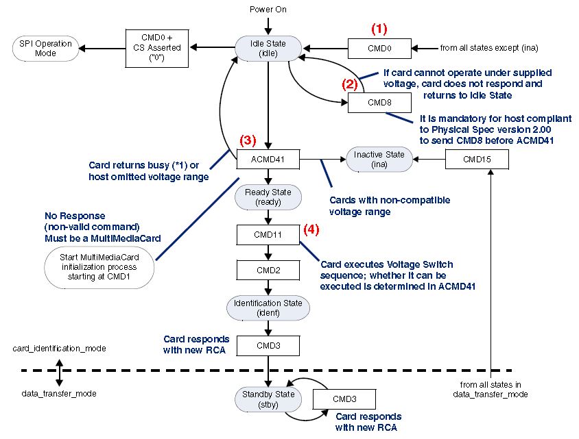
- Card executes internal initialization process†
- Card is High or Extended capacity SD Memory Card and host does not support High†
The following outlines the steps for the voltage switch programming sequence.†
- Software Driver starts CMD0, which selects the bus mode as SD.†
- After the bus is in SD card mode, CMD8 is started in order to verify if the card is compatible with the SD Memory Card Specification, Version 2.00.†
CMD8 determines if the card is capable of working within the host supply voltage specified in the VHS (19:16) field of the CMD; the card supports the current host voltage if a response to CMD8 is received.†
- ACMD 41 is started.†
The response to this command informs the software if the card supports voltage switching; bits 38, 36, and 32 are checked by the card argument of ACMD41.†Figure 75. ACMD41 Argument
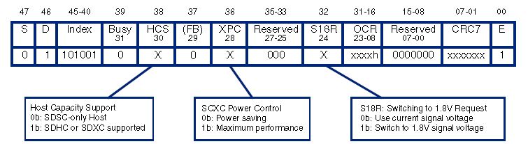
- Bit 30 informs the card if host supports SDHC/SDXC or not; this bit should be set to 1'b1.†
- Bit 28 can be either 1 or 0.†
- Bit 24 should be set to 1'b1, indicating that the host is capable of voltage switching.†
Figure 76. ACMD41 Response (R3)†
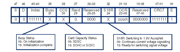
- Bit 30 – If set to 1'b1, card supports SDHC/SDXC; if set to 1'b0, card supports only SDSC.†
- Bit 24 – If set to 1'b1, card supports voltage switching and is ready for the switch.†
- Bit 31 – If set to 1'b1, initialization is over; if set to 1'b0, means initialization in process†
-
If the card supports voltage switching, then the software must perform the steps discussed for either the “Voltage Switch Normal Scenario” or the “Voltage Switch Error Scenario”, located in the Synopsys® DesignWare Cores Mobile Storage Host Databook.