Arria® 10 and Cyclone® 10 GX Avalon® Streaming Interface for PCI Express* User Guide
ID
683647
Date
9/11/2024
Public
1. Datasheet
2. Quick Start Guide
3. Arria® 10 or Cyclone® 10 GX Parameter Settings
4. Physical Layout
5. Interfaces and Signal Descriptions
6. Registers
7. Reset and Clocks
8. Interrupts
9. Error Handling
10. PCI Express Protocol Stack
11. Transaction Layer Protocol (TLP) Details
12. Throughput Optimization
13. Design Implementation
14. Additional Features
15. Hard IP Reconfiguration
16. Testbench and Design Example
17. Debugging
A. Transaction Layer Packet (TLP) Header Formats
B. Lane Initialization and Reversal
C. Arria® 10 or Cyclone® 10 GX Avalon-ST Interface for PCIe Solutions User Guide Archive
D. Document Revision History
3.1. Parameters
3.2. Arria® 10 or Cyclone® 10 GX Avalon-ST Settings
3.3. Base Address Register (BAR) and Expansion ROM Settings
3.4. Base and Limit Registers for Root Ports
3.5. Device Identification Registers
3.6. PCI Express and PCI Capabilities Parameters
3.7. Vendor Specific Extended Capability (VSEC)
3.8. Configuration, Debug, and Extension Options
3.9. PHY Characteristics
3.10. Example Designs
5.1. Avalon‑ST RX Interface
5.2. Avalon-ST TX Interface
5.3. Clock Signals
5.4. Reset, Status, and Link Training Signals
5.5. ECRC Forwarding
5.6. Error Signals
5.7. Interrupts for Endpoints
5.8. Interrupts for Root Ports
5.9. Completion Side Band Signals
5.10. Parity Signals
5.11. LMI Signals
5.12. Transaction Layer Configuration Space Signals
5.13. Hard IP Reconfiguration Interface
5.14. Power Management Signals
5.15. Physical Layer Interface Signals
5.1.1. Avalon-ST RX Component Specific Signals
5.1.2. Data Alignment and Timing for the 64‑Bit Avalon® -ST RX Interface
5.1.3. Data Alignment and Timing for the 128‑Bit Avalon‑ST RX Interface
5.1.4. Data Alignment and Timing for 256‑Bit Avalon‑ST RX Interface
5.1.5. Tradeoffs to Consider when Enabling Multiple Packets per Cycle
5.2.1. Avalon-ST Packets to PCI Express TLPs
5.2.2. Data Alignment and Timing for the 64‑Bit Avalon-ST TX Interface
5.2.3. Data Alignment and Timing for the 128‑Bit Avalon‑ST TX Interface
5.2.4. Data Alignment and Timing for the 256‑Bit Avalon‑ST TX Interface
5.2.5. Root Port Mode Configuration Requests
16.4.1. ebfm_barwr Procedure
16.4.2. ebfm_barwr_imm Procedure
16.4.3. ebfm_barrd_wait Procedure
16.4.4. ebfm_barrd_nowt Procedure
16.4.5. ebfm_cfgwr_imm_wait Procedure
16.4.6. ebfm_cfgwr_imm_nowt Procedure
16.4.7. ebfm_cfgrd_wait Procedure
16.4.8. ebfm_cfgrd_nowt Procedure
16.4.9. BFM Configuration Procedures
16.4.10. BFM Shared Memory Access Procedures
16.4.11. BFM Log and Message Procedures
16.4.12. Verilog HDL Formatting Functions
2.5. Compiling and Testing the Design in Hardware
Figure 11. Procedure
Figure 12. Software Application to Test the PCI Express Design Example on the Arria® 10 GX FPGA Development KitA software application running on a Windows PC performs the same hardware test for all of the PCI Express Design Examples.
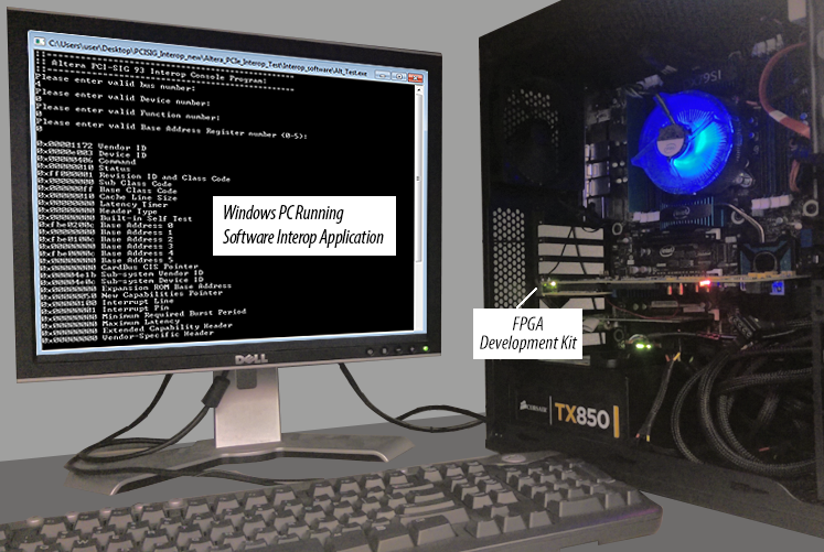
The software application to test the PCI Express Design Example on the Arria® 10 GX FPGA Development Kit is available on both 32- and 64-bit Windows 7 platforms. This program performs the following tasks:
- Prints the Configuration Space, lane rate, and lane width.
- Writes 0x00000000 to the specified BAR at offset 0x00000000 to initialize the memory and read it back.
- Writes 0xABCD1234 at offset 0x00000000 of the specified BAR. Reads it back and compares.
If successful, the test program displays the message 'PASSED'
Follow these steps to compile the design example in the Quartus Prime software:
- Launch the Quartus Prime software and open the pcie_example_design.qpf file for the example design created above.
- On the Processing > menu, select Start Compilation.
The timing constraints for the design example and the design components are automatically loaded during compilation.
Follow these steps to test the design example in hardware:
- In the <example_design>/software/windows/interop directory, unzip Altera_PCIe_Interop_Test.zip.
Note: You can also refer to readme_Altera_PCIe_interop_Test.txt file in this same directory for instructions on running the hardware test.
- Install the Intel® FPGA Windows Demo Driver for PCIe on the Windows host machine, using altera_pcie_win_driver.inf.
Note: If you modified the default Vendor ID (0x1172) or Device ID (0x0000) specified in the component parameter editor GUI, you must also modify them in altera_pcie_win_driver.inf.
- In the <example_design> directory, launch the Quartus Prime software and compile the design (Processing > Start Compilation).
- Connect the development board to the host computer.
- Configure the FPGA on the development board using the generated .sof file (Tools > Programmer).
- Open the Windows Device Manager and scan for hardware changes.
- Select the Intel® FPGA listed as an unknown PCI device and point to the appropriate 32- or 64-bit driver (altera_pice_win_driver.inf) in the Windows_driver directory.
- After the driver loads successfully, a new device named Altera PCI API Device appears in the Windows Device Manager.
- Determine the bus, device, and function number for the Altera PCI API Device listed in the Windows Device Manager.
- Expand the tab, Altera PCI API Driver under the devices.
- Right click on Altera PCI API Device and select Properties.
- Note the bus, device, and function number for the device. The following figure shows one example.
Figure 13. Determining the Bus, Device, and Function Number for New PCIe Device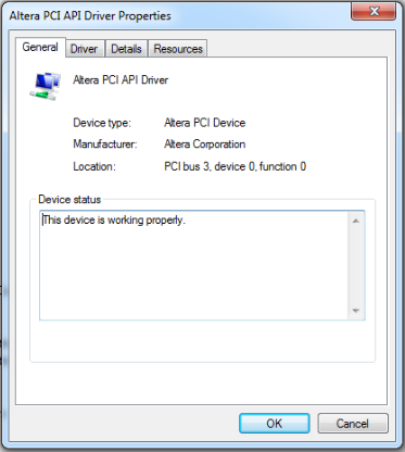
- In the <example_design>/software/windows/interop/Altera_PCIe_Interop_Test/Interop_software directory, click Alt_Test.exe.
- When prompted, type the bus, device, and function numbers and select the BAR number (0-5) you specified when parameterizing the IP core.
Note: The bus, device, and function numbers for your hardware setup may be different.
- The test displays the message, PASSED, if the test is successful.
Note: For more details on additional design implementation steps such as making pin assignments and adding timing constraints, refer to the Design Implementation chapter.