1. Transceiver Architecture in Arria V Devices
2. Transceiver Clocking in Arria V Devices
3. Transceiver Reset Control in Arria V Devices
4. Transceiver Protocol Configurations in Arria V Devices
5. Transceiver Custom Configurations in Arria V Devices
6. Transceiver Configurations in Arria V GZ Devices
7. Transceiver Loopback Support in Arria V Devices
8. Dynamic Reconfiguration in Arria V Devices
1.2.2.1.1. Word Aligner in Manual Alignment Mode
1.2.2.1.2. Bit-Slip Mode
1.2.2.1.3. Word Aligner in Automatic Synchronization State Machine Mode
1.2.2.1.4. Word Aligner in Deterministic Latency State Machine Mode
1.2.2.1.5. Programmable Run-Length Violation Detection
1.2.2.1.6. Receiver Polarity Inversion
1.2.2.1.7. Bit Reversal
1.2.2.1.8. Receiver Byte Reversal
3.1. PHY IP Embedded Reset Controller
3.2. User-Coded Reset Controller
3.3. Transceiver Reset Using Avalon Memory Map Registers
3.4. Clock Data Recovery in Manual Lock Mode
Resetting the Transceiver During Dynamic Reconfiguration
3.6. Transceiver Blocks Affected by the Reset and Powerdown Signals
3.7. Transceiver Power-Down
3.8. Document Revision History
3.2.1. User-Coded Reset Controller Signals
3.2.2. Resetting the Transmitter with the User-Coded Reset Controller During Device Power-Up
3.2.3. Resetting the Transmitter with the User-Coded Reset Controller During Device Operation
3.2.4. Resetting the Receiver with the User-Coded Reset Controller During Device Power-Up Configuration
3.2.5. Resetting the Receiver with the User-Coded Reset Controller During Device Operation
4.1. PCI Express
4.2. Gigabit Ethernet
4.3. XAUI
4.4. 10GBASE-R
4.5. Serial Digital Interface
4.6. Gigabit-Capable Passive Optical Network (GPON)
4.7. Serial Data Converter (SDC) JESD204
4.8. SATA and SAS Protocols
4.9. Deterministic Latency Protocols—CPRI and OBSAI
4.10. Serial RapidIO
4.11. Document Revision History
4.1.2.1. PIPE Interface
4.1.2.2. Transmitter Electrical Idle Generation
4.1.2.3. Power State Management
4.1.2.4. 8B/10B Encoder Usage for Compliance Pattern Transmission Support
4.1.2.5. Receiver Status
4.1.2.6. Receiver Detection
4.1.2.7. Clock Rate Compensation Up to ±300 ppm
4.1.2.8. PCIe Reverse Parallel Loopback
6.1.1. 10GBASE-R and 10GBASE-KR Transceiver Datapath Configuration
6.1.2. 10GBASE-R and 10GBASE-KR Supported Features
6.1.3. 1000BASE-X and 1000BASE-KX Transceiver Datapath
6.1.4. 1000BASE-X and 1000BASE-KX Supported Features
6.1.5. Synchronization State Machine Parameters in 1000BASE-X and 1000BASE-KX Configurations
6.1.6. Transceiver Clocking in 10GBASE-R, 10GBASE-KR, 1000BASE-X, and 1000BASE-KX Configurations
6.3.1. Transceiver Datapath Configuration
6.3.2. Supported Features for PCIe Configurations
6.3.3. Supported Features for PCIe Gen3
6.3.4. Transceiver Clocking and Channel Placement Guidelines
6.3.5. Advanced Channel Placement Guidelines for PIPE Configurations
6.3.6. Transceiver Clocking for PCIe Gen3
6.7.1. Protocols and Transceiver PHY IP Support
6.7.2. Native PHY Transceiver Datapath Configuration
6.7.3. Standard PCS Features
6.7.4. 10G PCS Supported Features
6.7.5. 10G Datapath Configurations with Native PHY IP
6.7.6. PMA Direct Supported Features
6.7.7. Channel and PCS Datapath Dynamic Switching Reconfiguration
8.1. Dynamic Reconfiguration Features
8.2. Offset Cancellation
8.3. Transmitter Duty Cycle Distortion Calibration
8.4. PMA Analog Controls Reconfiguration
8.5. Dynamic Reconfiguration of Loopback Modes
8.6. Transceiver PLL Reconfiguration
8.7. Transceiver Channel Reconfiguration
8.8. Transceiver Interface Reconfiguration
8.9. Reduced .mif Reconfiguration
8.10. On-Chip Signal Quality Monitoring (Eye Viewer)
8.11. Adaptive Equalization
8.12. Decision Feedback Equalization
8.13. Unsupported Reconfiguration Modes
8.14. Document Revision History
2.2.2.1. Non-Bonded Channel Configurations
The channel clock path for non-bonded configurations can be driven by the x1, or the x6 and xN clock lines.
| Clock Line | Transmitter PLL | Clock Path |
|---|---|---|
| x1 | ATX PLL23 | ATX PLL » x1 » individual clock divider » serializer |
| CMU | CMU PLL » x1 » individual clock divider » serializer | |
| fPLL | fPLL » x1_fPLL » individual clock divider » serializer | |
| x6, xN | ATX PLL23 | ATX PLL » central clock divider » x6 » xN » individual clock divider » serializer |
| CMU | CMU PLL » central clock divider » x6 » xN » individual clock divider » serializer 24 | |
| fPLL | fPLL » x1_fPLL » central clock divider » x6 » individual clock divider » serializer 24 |
Figure 55. Three Non-Bonded Transmitter Channels Driven by CMU PLL using x1 Clock Line Within a Transceiver Bank
Figure 56. Three Non-Bonded Transmitter Channels Driven by fPLL using x1 Clock Line Within a Transceiver Bank
Figure 57. Three Non-Bonded Transmitter Channels Driven by ATX PLL using x1 Clock Line Within a Transceiver Bank for GZ Devices.
Figure 58. Three Non-Bonded Transmitter Channels Driven by CMU PLL using x6 and xN Clock Lines Across Multiple Transceiver Banks
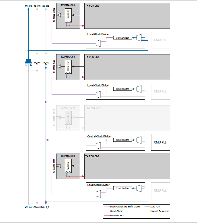
Figure 59. Three Non-Bonded Transmitter Channels Driven by fPLL using x6 and xN Clock Line Across Multiple Transceiver Banks
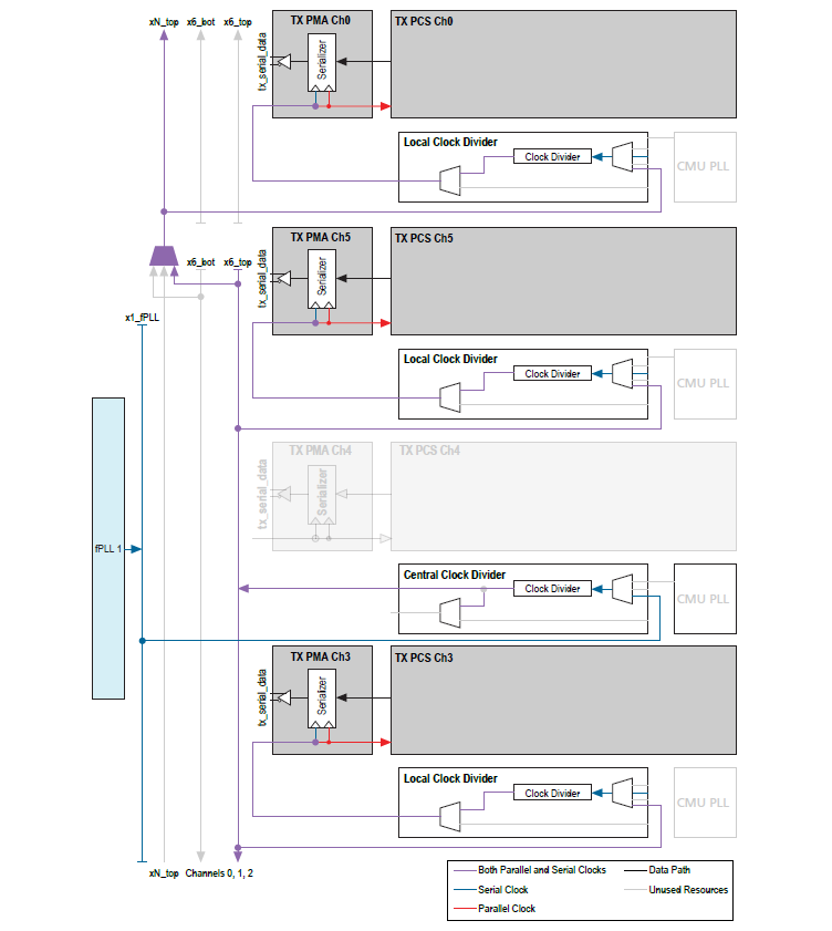
When the fPLL is used to drive more than three non-bonded channels, the channel where the central clock divider resides adjacent to the fPLL cannot be used as a transmitter. The fPLL uses a central clock divider to access the x6 clock network when driving more than three non-bonded channels, so the divider is no longer available to implement a transmitter. For xN non-bonded configurations, the ch 1 or ch 4 transceiver bank where the central clock divider resides cannot be used as a data channel since the parallel clock cannot be generated in this channel.
23 ATX PLL is available only for GZ devices.
24 Non-bonded channels within same bank as TX PLL are driven by clocks from x6 clock line, and channels in other banks are driven from xN clock line.