External Memory Interfaces Intel Agilex® 7 M-Series FPGA IP User Guide
A newer version of this document is available. Customers should click here to go to the newest version.
3.1.3. Intel Agilex® 7 M-Series EMIF Architecture: I/O Bank
Each I/O bank consists of two sub-banks, and each sub-bank contains the following components:
- I/O PLL and PHY clock trees
- DLL
- Input DQS clock trees
- 48 pins, organized into four I/O lanes of 12 pins each

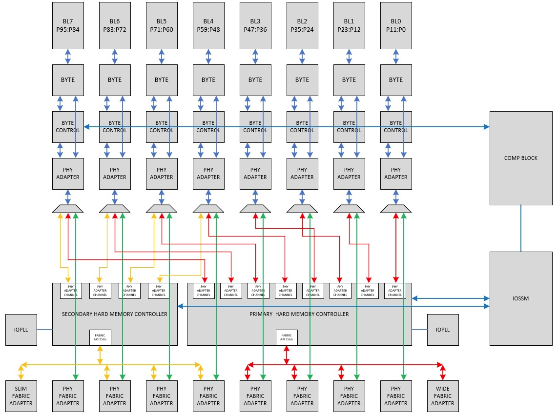
Within an I/O bank, the top sub-bank is pin indexes P95:P48, and the bottom sub-bank is pin indexes P47:P0.
Intel Agilex® 7 M-Series devices have two hard memory controllers: primary and secondary. The primary hard memory controller has access to all 96 pins in an I/O bank. The secondary hard memory controller has access only to the top sub-bank. In the above figure, the yellow signals highlight the connections for the secondary hard memory controller, while the red signals show the connections for the primary hard memory controller. The green signals show where both hard memory controllers are bypassed to provide access to the PHY from the core logic.