External Memory Interfaces Intel Agilex® 7 M-Series FPGA IP User Guide
ID
772538
Date
6/26/2023
Public
A newer version of this document is available. Customers should click here to go to the newest version.
1. About the External Memory Interfaces Intel Agilex® 7 M-Series FPGA IP
2. Intel Agilex® 7 M-Series FPGA EMIF IP – Introduction
3. Intel Agilex® 7 M-Series FPGA EMIF IP – Product Architecture
4. Intel Agilex® 7 M-Series FPGA EMIF IP – End-User Signals
5. Intel Agilex® 7 M-Series FPGA EMIF IP – Simulating Memory IP
6. Intel Agilex 7 M-Series FPGA EMIF IP – DDR4 Support
7. Intel Agilex® 7 M-Series FPGA EMIF IP – DDR5 Support
8. Intel Agilex 7 M-Series FPGA EMIF IP – LPDDR5 Support
9. Intel Agilex® 7 M-Series FPGA EMIF IP – Timing Closure
10. Intel Agilex® 7 M-Series FPGA EMIF IP – Controller Optimization
11. Intel Agilex® 7 M-Series FPGA EMIF IP – Debugging
12. Document Revision History for External Memory Interfaces Intel Agilex® 7 M-Series FPGA IP User Guide
3.1.1. Intel Agilex® 7 M-Series EMIF Architecture: I/O Subsystem
3.1.2. Intel Agilex® 7 M-Series EMIF Architecture: I/O SSM
3.1.3. Intel Agilex® 7 M-Series EMIF Architecture: I/O Bank
3.1.4. Intel Agilex® 7 M-Series EMIF Architecture: I/O Lane
3.1.5. Intel Agilex® 7 M-Series EMIF Architecture: Input DQS Clock Tree
3.1.6. Intel Agilex® 7 M-Series EMIF Architecture: PHY Clock Tree
3.1.7. Intel Agilex® 7 M-Series EMIF Architecture: PLL Reference Clock Networks
3.1.8. Intel Agilex® 7 M-Series EMIF Architecture: Clock Phase Alignment
3.1.9. User Clock in Different Core Access Modes
6.2.4.1. Address and Command Pin Placement for DDR4
6.2.4.2. DDR4 Data Width Mapping
6.2.4.3. General Guidelines - DDR4
6.2.4.4. x4 DIMM Implementation
6.2.4.5. Specific Pin Connection Requirements
6.2.4.6. Command and Address Signals
6.2.4.7. Clock Signals
6.2.4.8. Data, Data Strobes, DM/DBI, and Optional ECC Signals
6.3.5.1. Single Rank x 8 Discrete (Component) Topology
6.3.5.2. Single Rank x 16 Discrete (Component) Topology
6.3.5.3. ADDR/CMD Reference Voltage/RESET Signal Routing Guidelines for Single Rank x 8 and Single Rank x 16 Discrete (Component) Topologies
6.3.5.4. Skew Matching Guidelines for DDR4 Discrete Configurations
6.3.5.5. Power Delivery Recommendations for DDR4 Discrete Configurations
6.3.5.6. Intel Agilex® 7 M-Series EMIF Pin Swapping Guidelines
7.2.1. Intel Agilex® 7 M-Series FPGA EMIF IP Interface Pins
7.2.2. Intel Agilex® 7 M-Series FPGA EMIF IP Resources
7.2.3. Pin Guidelines for Intel Agilex® 7 M-Series FPGA EMIF IP
7.2.4. Pin Placements for Intel Agilex 7 M-Series FPGA DDR5 EMIF IP
7.2.5. Intel Agilex® 7 M-Series EMIF Pin Swapping Guidelines
6.3.5.2. Single Rank x 16 Discrete (Component) Topology
Five memory devices are required to cover 72 bits of data in a single channel, with one rank and ×16 memory devices.
The interface covers data bytes (DQ/DQS), address signals, command signals (BA, BG, RAS, CAS, WE, ACT, PAR), control signals (CKE, CS, ODT) and clocks (CLK).
Figure 27. Signal connections for DDR4 Single Rank × 16 Discrete Topology (5 memory devices to cover 72 bits)

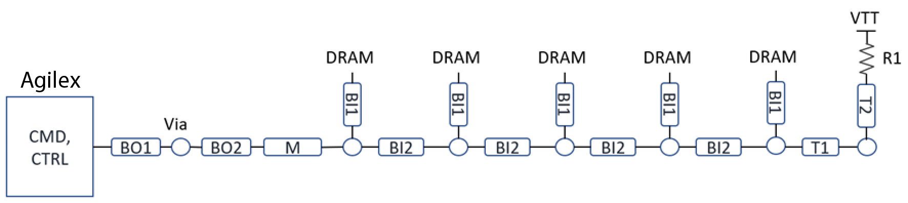
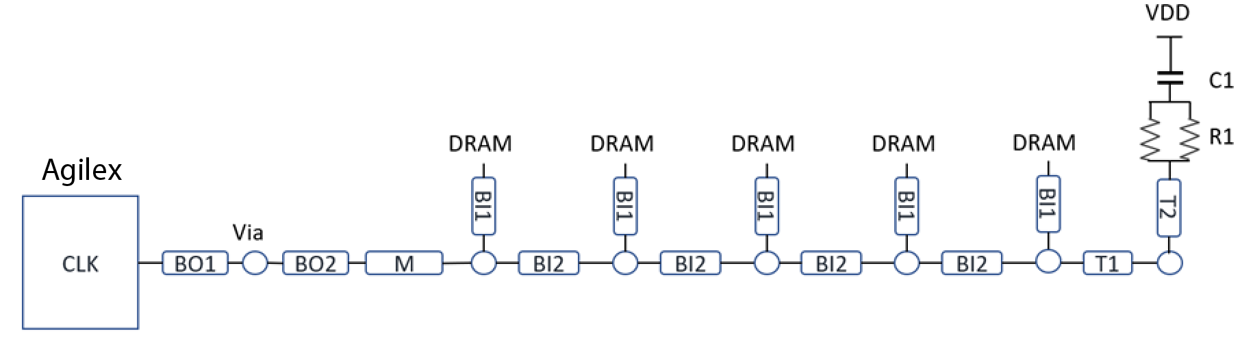
| Signal Group | Segment | Routing Layer | Max Length (mil) | Target Zse (ohm) | Trace Width, W (mil) | Trace Spacing, S1 (mil): Within Group | Trace Spacing, S2 (mil): CMD/CTRL/CLK to DQ/DQS | Trace Spacing, S3 (mil): DQ Nibble to Nibble | Trace Spacing (mil), Within DIFF pair | Trace Spacing (mil), DQS pair to DQ | Trace Spacing (mil), CLK pair to CMD/CTRL/CKE | Rtt / Ctt | |
|---|---|---|---|---|---|---|---|---|---|---|---|---|---|
| Segment | Total MB | ||||||||||||
| CLK | BO1 | US | 50 | To first DRAM: 4000. To last DRAM: 6800. | 4 | 5, 17 | 17 | 4 | 17 | R1=36Ω. C1=10nF | |||
| BO2 | SL | 1000 | 4 | 5, 17 | 17 | 4 | 17 | ||||||
| M | SL | 40 | 5.5 | 12 (3h) | 4 | 12 (3h) | |||||||
| BI1 | US | 50 | 3 | 12 (3h) | 4 | 12 (3h) | |||||||
| BI2 | SL | 700 | 50 | 3 | 12 (3h) | 4 | 12 (3h) | ||||||
| T1 | SL | 300 | 3 | 12 (3h) | 4 | 12 (3h) | |||||||
| T2 | US | 50 | 3 | 12 (3h) | 4 | 12 (3h) | |||||||
| CMD, CTRL, Alert | BO1 | US | 50 | To first DRAM: 4000. To last DRAM: 6800. | 4 | 5, 17 | 17 | R1=36Ω alert_n requires an external pullup resistor to VDD (1.2V) of approximately 1KΩ. | |||||
| BO2 | SL | 1000 | 4 | 5, 17 | 17 | ||||||||
| M | SL | 40 | 5.5 | 8 (2H) | 12 (3h) | ||||||||
| BI1 | US | 50 | 3 | 8 (2H) | 12 (3h) | ||||||||
| BI2 | SL | 700 | 50 | 3 | 8 (2H) | 12 (3h) | |||||||
| T1 | SL | 300 | 3 | 8 (2H) | 12 (3h) | ||||||||
| T2 | US | 50 | 3 | 8 (2H) | 12 (3h) | ||||||||
| DQ | BO1 | US | 50 | 5000 | 4 | 5, 17 | 17 | ||||||
| BO2 | SL | 1000 | 4 | 5, 17 | 17 | ||||||||
| M | SL | 45 | 4.5 | 8 (2H) | 12 (3h) | ||||||||
| BI | US | 50 | 4 | 8 (2H) | 12 (3h) | ||||||||
| DQS | BO1 | US | 50 | 5000 | 4 | 4 | 17 | ||||||
| BO2 | SL | 1000 | 4 | 4 | 17 | ||||||||
| M | SL | 45 | 4.5 | 4 | 12 (3h) | ||||||||
| BI | US | 50 | 4 | 4 | 12 (3h) | ||||||||
| For an explanation of the guidelines represented in this table, refer to the bullet points immediately following Figure 22. | |||||||||||||