External Memory Interfaces Arria® 10 FPGA IP User Guide
3.7.1. Restrictions on I/O Bank Usage for Arria® 10 EMIF IP with HPS
The restrictions on I/O bank usage result from the Arria® 10 HPS having hard-wired connections to the EMIF circuits in the I/O banks closest to the HPS. For any given EMIF configuration, the pin-out of the EMIF-to-HPS interface is fixed.
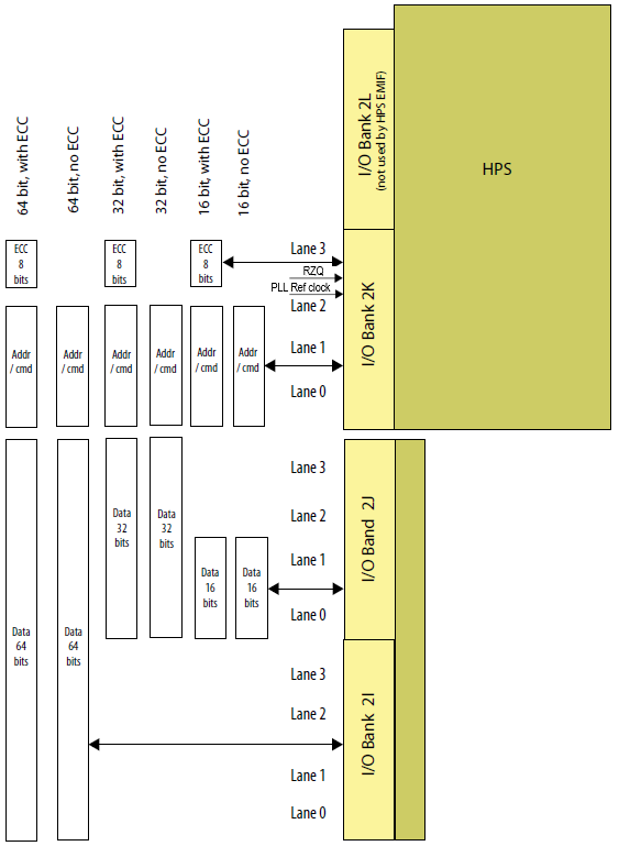
The following diagram illustrates the use of I/O banks and lanes for various EMIF-HPS data widths:
You should refer to the pinout file for your device and package for detailed information. Banks and pins used for HPS access to a DDR interface are labeled HPS_DDR in the HPS Function column of the pinout file.
By default, the Arria® 10 External Memory Interface for HPS IP core together with the Quartus® Prime Fitter automatically implement the correct pin-out for HPS EMIF without you having to implement additional constraints. If, for any reason, you must modify the default pin-out, you must adhere to the following requirements, which are specific to HPS EMIF:
- Within a single data lane (which implements a single x8 DQS group):
- DQ pins must use pins at indices 1, 2, 3, 6, 7, 8, 9, 10. You may swap the locations between the DQ bits (that is, you may swap location of DQ[0] and DQ[3]) so long as the resulting pin-out uses pins at these indices only.
- DM/DBI pin must use pin at index 11. There is no flexibility.
- DQS/DQS# must use pins at index 4 and 5. There is no flexibility.
- Assignment of data lanes must be as illustrated in the above figure. You are allowed to swap the locations of entire byte lanes (that is, you may swap locations of byte 0 and byte 3) so long as the resulting pin-out uses only the lanes permitted by your HPS EMIF configuration, as shown in the above figure.
- You must not change placement of the address and command pins from the default.
- You may place the alert# pin at any available pin location in either a data lane or an address and command lane.
- The PLL reference clock must be placed in I/O bank 2K with the address and command pins.
- The RZQ pin must be placed in I/O bank 2K with the address and command pins.
To override the default generated pin assignments, comment out the relevant HPS_LOCATION assignments in the .qip file, and add your own location assignments (using set_location_assignment) in the .qsf file.
When the HPS is connected to external SDRAM memory, no other Arria® 10 External Memory Interface IP instances can be placed in the same I/O column.
Guideline: Using the I/O Pins in HPS Shared I/O Banks
Arria® 10 SX devices have 3 modular I/O banks (2K, 2J, and 2I) that connect the HPS to an SDRAM through a dedicated HPS EMIF. Each bank has 4 I/O lanes that correspond as follows:
- Lane 3: IO[47:36]
- Lane 2: IO[35:24]
- Lane 1: IO[23:12]
- Lane 0: IO[11:0]
When there is no HPS EMIF in the system, the entire HPS EMIF bank can be used as FPGA general purpose I/Os (GPIOs). However, when there is an HPS EMIF in the system, adhere to the following guidelines for the usage of unused HPS EMIF pins:
- Bank 2K, lane 3 is used for ECC signals of the SDRAM. You can use unused pins in this lane as FPGA inputs only.
- Bank 2K, lanes 2, 1, and 0 are used for Address and Command signals of the SDRAM. You can use unused pins in these lanes as both FPGA inputs or outputs.
- Bank 2J is used for Data signals [31:0] while bank 2I is used for Data signals [63:32] of the SDRAM.
- When using 16-bit data width, unused pins in the 2 lanes of bank 2J used for data can be used as FPGA inputs only. The pins in the remaining 2 lanes of bank 2J and all of bank 2I can be used as both FPGA inputs or outputs.
- When using 32-bit data width, unused pins in bank 2J can be used as FPGA inputs only. Pins in bank 2I can be used as both FPGA inputs or outputs.
- When using 64-bit data width, unused pins in banks 2J and 2I can be used as FPGA inputs only.