10.3.1. Native Floating Point DSP Stratix® 10 FPGA IP Parameters
| Parameter | Value | Default Value | Description |
|---|---|---|---|
| DSP Template | Multiply Add Multiply Add Multiply Accumulate Vector Mode 1 Vector Mode 2 |
Multiply | Select the desired operational mode for the DSP block. The selected operation is reflected in the DSP Block View. |
| View | Register Enables Register Clears |
Register Enables | Options to select clocking scheme or reset scheme for registers view. The selected operation is reflected in the DSP Block View. Select Register Enables for DSP Block View to show registers clocking scheme. You can change the clocks for each of the registers in this view. Select Register Clears for DSP Block View to show registers reset scheme. Turn on Use Single Clear to change the registers reset scheme. |
| Clear Type | None Synchronous Asynchronous |
Synchronous | Options to select reset type for all registers. Select None to not reset the registers. Select Synchronous use synchronous clear signal type for all registers. Select Asynchronous to use asynchronous clear signal type for all registers. |
| Single Clear | On or off | Off | Turn on this parameter if you want a single reset to reset all the registers in the DSP block. Turn off this parameter to use different reset ports to reset the registers. This parameter is disable when you select None for Clear Type. |
| Connect Exception Flags | On Off |
Off | Click this parameter to use and generate exception flags output ports for the DSP block. When you turn off this parameter, the IP core does not generate exception flags output ports. |
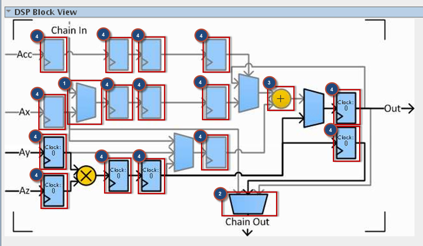
| DSP View Block. | |||
| Chain In Multiplexer (1) | Enable Disable |
Disable | Click the multiplexer to enable chainin port. |
| Chain Out Multiplexer (2) | Disable Enable |
Disable | Click the multiplexer to enable chainout port. |
| Adder (3) | + - |
+ | Click the Adder symbol to select addition or subtraction mode. |
| Register Clock (4) | None Clock 0 Clock 1 Clock 2 |
Clock 0 | To bypass any register, switch the register clock to None.
Switch the register clock to:
You can only change these settings when you select Register Enables in View parameter. |
| Register Clear (4) | Clear 0 Clear 1 |
Clear 0 for input registers Clear 1 for output and pipeline registers |
This view shows the IP core reset scheme. Clear 0 uses clr[0] signal. Clear 1 uses clr[1] signal. All input registers use clr[0] reset signal. All output and pipeline registers use clr[1] reset signal. |